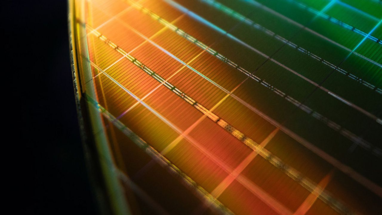
Imagine trying to build a tower out of hundreds of very thin, slightly different sheets of material, where each sheet wants to bend or warp on its own. That’s essentially what researchers at imec and Ghent University accomplished when they grew 120 alternating layers of silicon (Si) and silicon-germanium (SiGe) on a 300 mm wafer—a key step toward three-dimensional DRAM. At first glance, it sounds like stacking sheets of paper; in reality, it’s more like balancing a house of cards with materials that naturally want to pull apart.
The challenge starts with lattice mismatch. Silicon and silicon-germanium crystals have slightly different atomic spacings, so when stacked, the layers naturally want to stretch or compress. Think of it like trying to stack a deck of cards where every second card is slightly larger than the first—without careful alignment, the stack warps and topples. In semiconductor terms, these “topples” appear as misfit dislocations, tiny defects that can ruin a memory chip’s performance.