
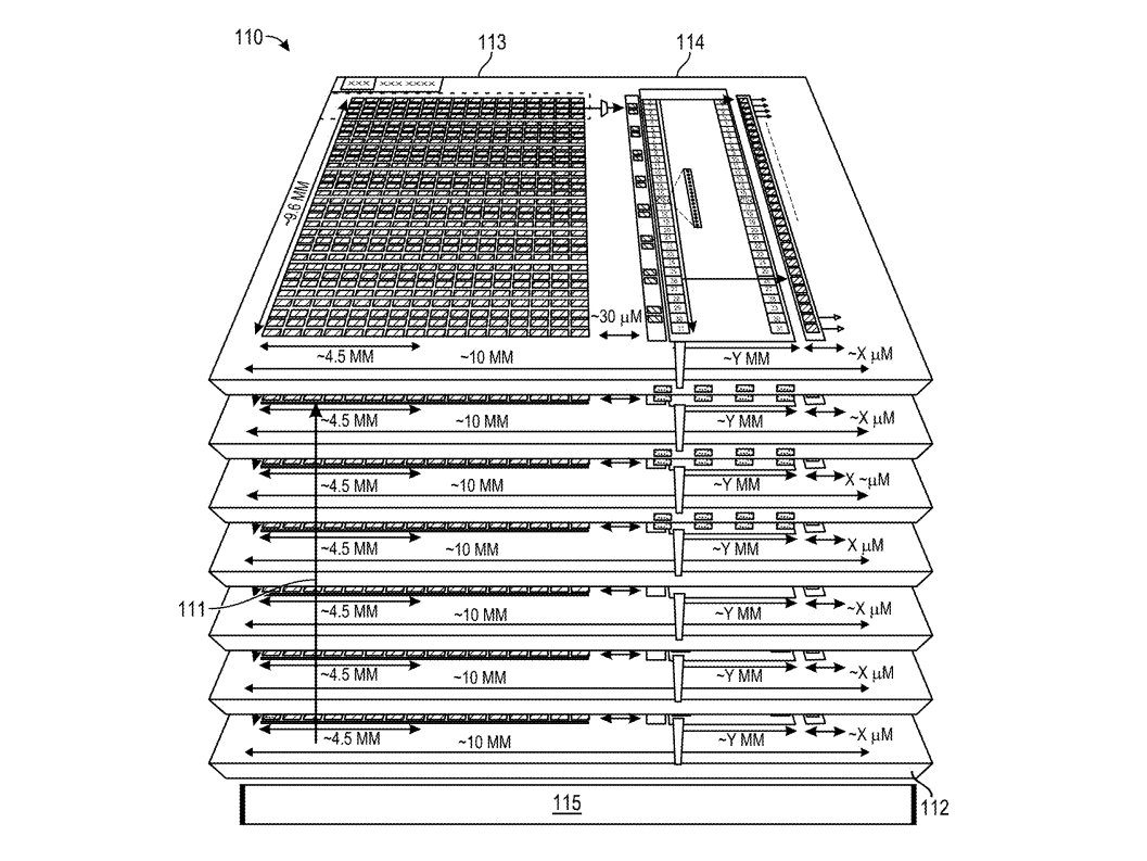
An Intel patent application published on July 2, 2026, surfaced by Underfox, has revealed the company's plans for a new high-bandwidth memory (HBM) architecture that aims to ease the packaging and cost bottleneck of today's interposer-based HBM. The patent application — filed back on December 26, 2024 — describes what Intel calls cross-batch memory (XBM), an "ultra-high-bandwidth memory with backend transistors" built with the goal of matching HBM4's footprint while swapping conventional DRAM and its ultra-wide interface for back-end-of-line (BEOL) transistors and serial Universal Chiplet Interconnect Express (UCIe) links.
Intel's proposed design is a memory stack that addresses the assembly costs that make conventional HBM expensive by dropping the costly silicon interposer and shrinking the package, while building in its own defect repair.