
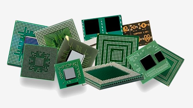
As the chip industry develops more sophisticated processors with higher heat dissipation requirements, some firms have moved on to chiplet-based designs. This not-so-gradual shift has resulted in chip packaging technologies becoming increasingly important. Large and highly complex chips such as Nvidia's H100 and advanced multi-chip solutions like Intel's Data Center Max GPU (Ponte Vecchio) present new requirements for packaging materials. To that end, Dai Nippon Printing (DNP) is showcasing a new development for semiconductor packages – Glass Core Substrate (GCS) – which it says can address many of those challenges.
Typically, modern chips are installed on fine pitch substrates (FPS), which are then put on multi-layer high-density interconnect (HDI) substrates. The most advanced CPU/GPU HDI substrates these days use Ajinomoto Build-up Film(ABF), which combines organic epoxy resins, hardener, and inorganic microparticle filler, according to the manufacturer. It is easy to use, and it can achieve high-density pitching (thus enabling high density metal wiring), it has insulation properties that are good enough for modern chips, high rigidity, high durability, and low thermal expansion, among other factors.