
Get all your news in one place.
100's of premium titles.
One app.
Start reading
Laptop
Laptop
Technology
Madeline Ricchiuto

Moore's law isn't dead — it's just buried under six feet of silicon spin

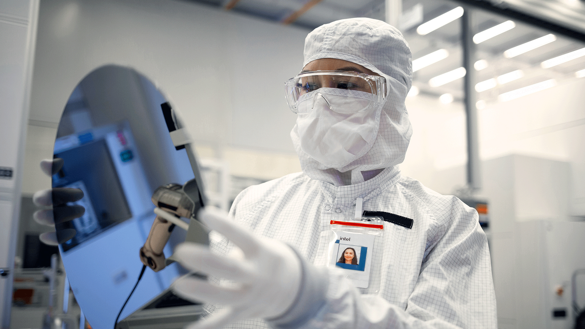
An Intel Foundry engineer in clean room gear holds a silicon wafer at an Intel facility in Chandler, Arizona.

Silicon wafer sizes aren't what you think, and those impossibly small "3nm" and "2nm" chips you keep hearing about? They're more marketing label than measurement.

The latest predictions by the Interuniversity Microelectronics Centre (IMEC), recently broken down by YouTuber TechTechPotato, presents the current timeline for TSMC's 2nm chipsets, as well as Intel Foundry's 18A and 14A process technologies, with A14 (1.4nm) chips expected in 2027 and A10 (1nm) process nodes expected in 2029. IMEC's predictions even highlight the possibility of producing 0.2mm silicon as early as 2039.

Sign up to read this article
Read news from 100's of titles, curated specifically for you.
Already a member? Sign in here
Related Stories
Top stories on inkl right now
One subscription that gives you access to news from hundreds of sites
Already a member? Sign in here
Our Picks
Fourteen days free
Download the app
One app. One membership.
100+ trusted global sources.