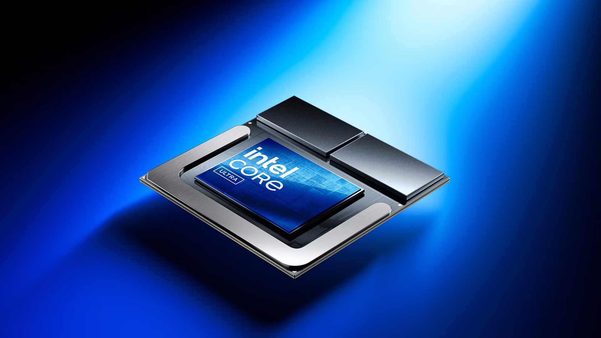
Die shots of Intel’s latest Core Ultra 200V (codenamed Lunar Lake) CPUs have been analyzed and annotated, revealing the size and location of the mobile chip’s components.
Photographed by GeekerWan and 万扯淡 and annotated by hardware expert Nemez, the images deeply dive into Lunar Lake’s tiniest parts in the compute, platform controller, and base tiles. The first two tiles are fabbed on TSMC’s 3nm and 6nm nodes, respectively, while the base tile alone is fabbed at Intel on the 22nm node.
Lunar Lake is oriented towards laptops. The quad-core Lion Cove P-core cluster, the NPU, and the Xe2 integrated GPU are all the same size. The media engine, display engine, and memory controller are smaller, unlike in higher-end processors, where they’re almost a footnote in size.
Annotation of #Intel LunarLake!Not much to highlight imo, though I quite like the layout of the iGPU, way less messy than MeteorLakeLionCove is also quite compact relative to its L2 cache compared to RedwoodCovePictures by GeekerWan & 万扯淡, provided to me by @Kurnalsalts pic.twitter.com/YVqqt8gRtsOctober 3, 2024
Lunar Lake also has a quad-core cluster of Skymont-based E-cores, and the die annotation indicates that the entire cluster is just a little larger than a single Lion Cove core. This isn’t surprising since Meteor Lake’s Redwood Cove P-core is about the same size as its quad-core Crestmont E-core cluster. However, it is notable that Intel was able to keep E-cores small despite Skymont packing 38% higher integer and 68% higher floating point IPC.
Some parts of the annotation are guesses made clear by the handful of question marks accompanying some labels. The amount of cache per neural compute engine (NCE) is also an educated guess, as Nemez assumes Lunar Lake is 2MB per NCE, just like Meteor Lake, for 12MB from six NCEs.
The platform controller tile isn’t quite as busy as the compute tile, but the annotation does give us a pretty good idea of how much more extensive PCIe 5.0 circuitry is compared to PCIe 4.0, as Lunar Lake has four lanes of both connections. It seems the four PCIe 5.0 lanes plus their logic take up roughly double the space that the PCIe 4.0 lanes and logic use. In addition to PCIe 5.0 SSDs not quite being laptop friendly yet, the physical size of PCIe 5.0 within silicon could be another reason mobile CPUs have taken so long to upgrade to the most recent PCIe version.


