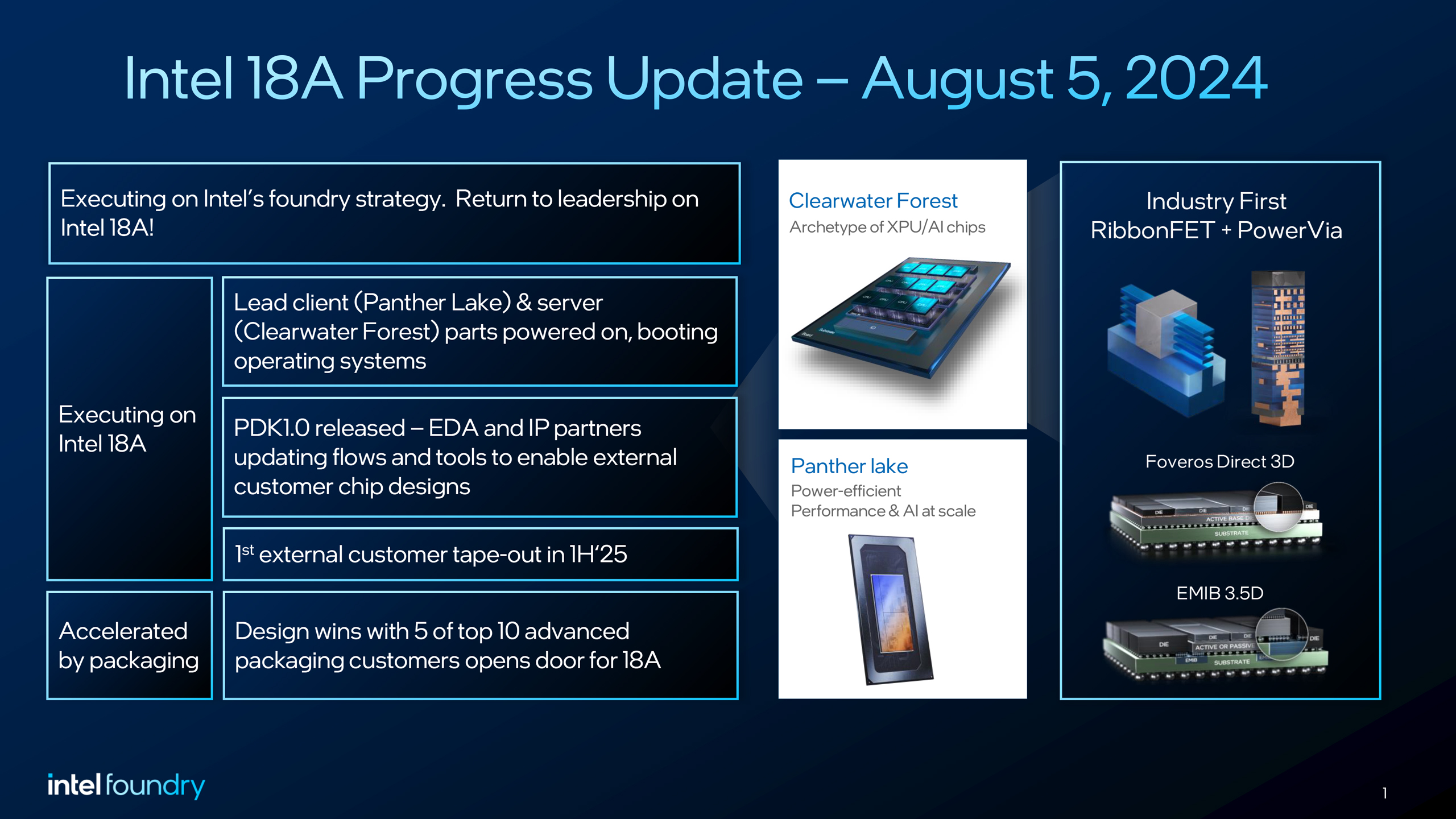
On Tuesday, Intel provided an update on the progress of its 18A (1.8nm-class) fabrication process, a crucial technology for its foundry initiative. By now, the company has a process design kit (PDK) version 1.0 ready, so its third-party customers can start (or even finalize) the development of chips in this manufacturing process. Furthermore, two essential Intel products using this production node have powered on, which is a good sign.
"The Panther Lake client processor is powered on and booting Windows, yielding well, in use inside Intel and ahead of schedule on product qualification milestones," said Kevin O'Buckley, Intel senior vice president and general manager of Foundry Services. "Clearwater Forest [CPU] for datacenter is powered on, booting operating systems, in use inside Intel and performing well."
Intel's 18A is the company's second fabrication technology to use gate-all-around RibbonFET transistors and backside power delivery called PowerVia (particularly crucial for data center-class products that need a lot of power) after 20A. Compared to the 2nm-class manufacturing process, 18A promises optimized RibbonFET design and some other enhancements, which leads to a 10% improvement in performance per watt.

Perhaps more important is that Intel 18A is a process that Intel Foundry's potential customers are very interested in, as it is believed to be more competitive than TSMC's 3nm and 2nm-class offerings available in 2024 – 2025. As a result, it is crucially vital for Intel and its ecosystem partners, such as Ansys, Cadence, Synopsys, and Siemens EDA, to adjust their tools for PDK 1.0 so as to enable Intel's lead customers to finalize their 18A designs that are currently in development and other clients to begin developing their 18A products.
"Ecosystem partners are updating EDA and IP process flows and tools to the Process Design Kit (PDK) 1.0, which will enable customers to begin their final production designs," said O'Buckley. "We are seeing continued interest from external foundry customers who are actively designing on Intel 18A. These positive outcomes are a signal for fabless customers and the industry at large that IDM 2.0 and our systems foundry strategy is working."
Intel expects its first external customer to tape out its first 18A design in the first half of 2025, so expect that design (assuming it is free of bugs and defects) to enter high-volume production in the first half of 2026. It means that Intel's 18A will be a little behind TSMC's N2 (a 2nm-class technology), which is set to be used for high-volume manufacturing in the second half of 2025.


