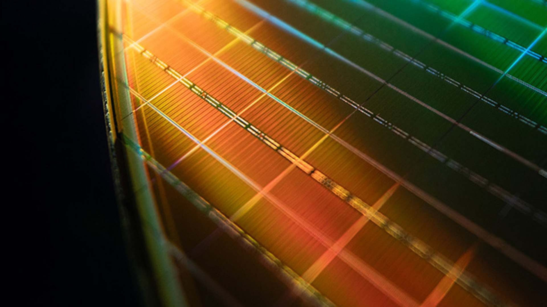
Scientists at the University of Massachusetts Amherst have introduced a novel method for aligning layers in chips using lasers and metalenses. The new technique is claimed to achieve accuracy down to the atomic scale, reports SciTechDaily. This advancement could be critical for next generation process technologies as well as integration of multi-chiplet 3D designs.
Overlay accuracy — precise alignment of one layer of a chip with the underlying layer — is one of the most critical capabilities of today's chipmaking tools as each wafer with logic chips requires over 4,000 manufacturing steps performed by different machines. Contemporary chipmaking tools perform overlay operations primarily using advanced optical metrology, alignment marks, and closed-loop control systems integrated into photolithography systems.