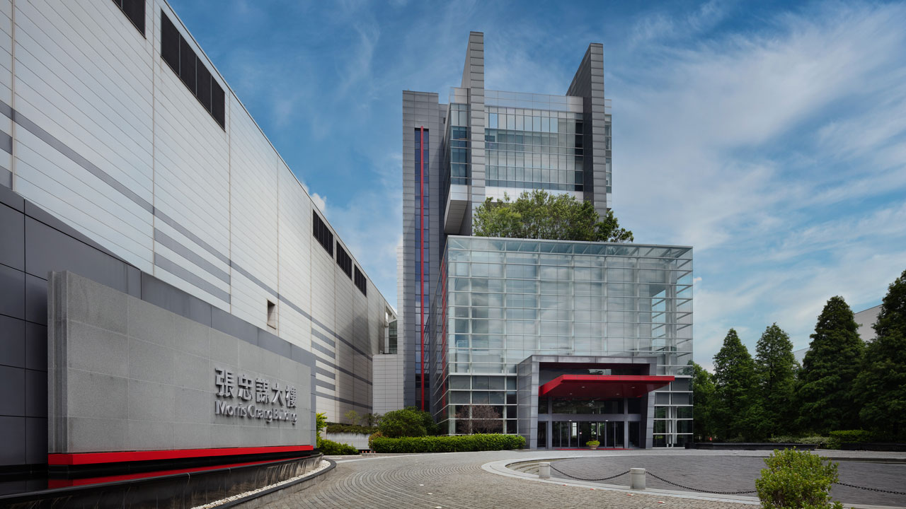
TSMC will host a formal opening ceremony for its first fab in Japan on February 24, 2024, new reports say. The semiconductor production facility will be capable of making chips using TSMC's N28 (28nm-class) technologies -- and will be the most advanced logic fab in the Land of the Rising Sun.
TSMC's Japanese fab will be located near Kumamoto, a city on the Japanese island of Kyushu, China Times reports citing Japanese media sources. The semiconductor manufacturing facility is set to process wafers using a variety of production nodes derived from the company's N28 (28nm-class) technology. This includes several N28 variants and the 22ULP fabrication process, a specialty node for ultra-low-power applications. While these manufacturing technologies are too outdated for use in advanced system-on-chips (SoCs) for smartphones or PCs, not to mention high-performance CPUs or GPUs, they are adequately suited for components used in the automotive and consumer electronics sectors. There remains a lot of demand for such processors in Japan with its multitude of sizable companies operating in these sectors.