Earlier this year SK hynix and TSMC announced a collaboration to develop and build base dies for HBM4 memory, but refrained from revealing any official details. At the European Technology Symposium 2024 this week, TSMC said that it would build HBM4 base dies using its 12FFC+ (12nm-class) and N5 (5nm-class) process technologies, reports AnandTech. The use of such advanced nodes will enable HBM4 to offer unprecedented performance and energy efficiency.
"We are working with key HBM memory partners (Micron, Samsung, SK hynix) over advanced nodes for HBM4 full stack integration," said the Senior Director of Design and Technology Platform at TSMC. "12FFC+ cost effective base die can reach HBM for performance and N5 base die can provide even more logic with much lower power at HBM4 speeds."
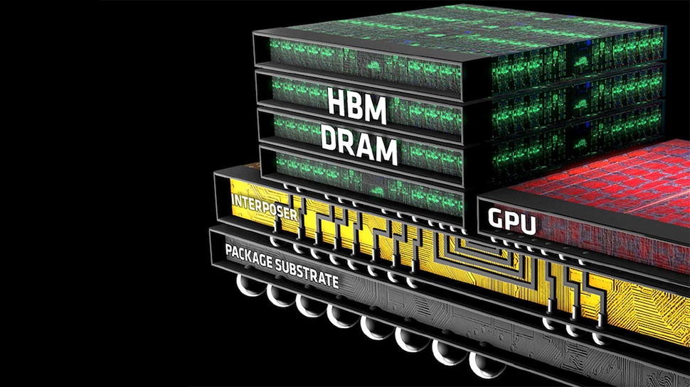
TSMC's N5 process technology is currently one of the most advanced production nodes available. It is used to make some of the best CPUs and best GPUs, so using it for memory is a big deal. What such an advanced node allows is to pack more logic and features into the HBM4 base die as well as enable very fine interconnection pitches (we are talking about pitches from 9 to 6 microns), which are essential for direct bonding on logic chips, thus boosting memory performance for AI and HPC processors.
Base dies made on TSMC's 12FFC+ process (derived from the company's established 16nm FinFET technology) will enable to build 12-Hi and 16-Hi HBM4 memory stacks that will offer capacities of 48 GB and 64 GB, respectively. Use of 12FFC+ will enable 'cost effective' base dies that will use silicon interposers to connect memory to host processors.
TSMC's Production Nodes for HBM4 Base Dies
TSMC is also optimizing its packaging technologies, particularly CoWoS-L and CoWoS-R, to support HBM4 integration. These advanced packaging methods enable the building of interposers of up to eight reticle sizes and facilitate the assembly of up to 12 HBM4 memory stacks. New interposers will feature up to eight layers to ensure efficient routing of more than 2,000 interconnects while maintaining proper signal integrity. By now, experimental HBM4 memory stacks have reached data transfer rates of 6 GT/s at 14mA, according to a TSMC slide.
"We are also optimizing CoWoS-L and CoWoS-R for HBM4," the TSMC representative said. "Both CoWoS-L and CoWoS-R [use] over eight layers to enable HBM4's routing of over 2,000 interconnects with [proper] signal integrity. We collaborate with EDA partners like Cadence, Synopsys, and Ansys to certify HBM4 channel signal integrity, IR/EM, and thermal accuracy."
TSMC's collaborative efforts with leading memory producers like Micron, Samsung, and SK hynix, as well as EDA partners including Cadence, Synopsys, and Ansys, are crucial to enable HBM4 memory subsystems a few years down the road.