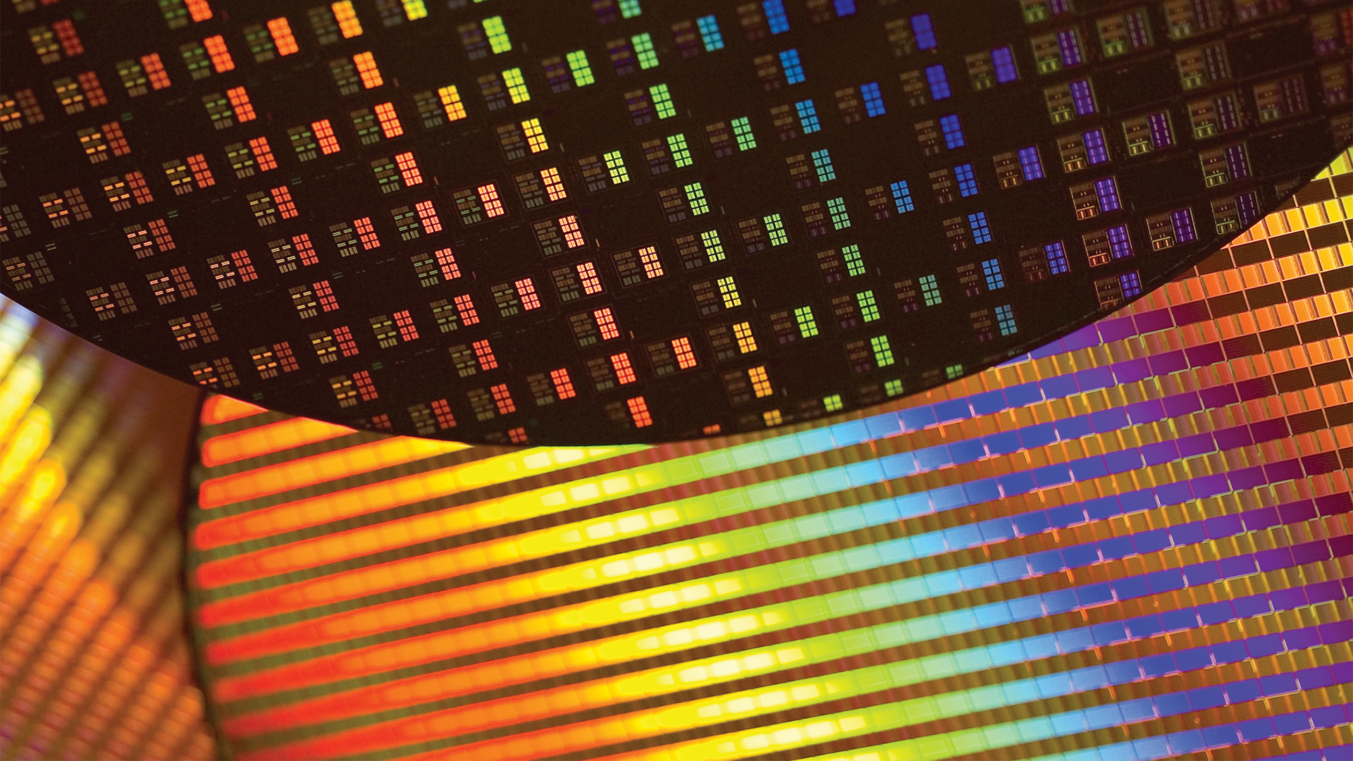
TSMC is set to start mass production of semiconductors using its N2 (2nm-class) fabrication process sometime in the second half of next year and right now the company is doing its best to polish off the technology in terms of lowering variability and defect density and therefore improving yields. As one of TSMC employees said recently, the team has managed to increase yields of test chips by 6%, 'creating billions in savings' for the company's customers.
The TSMC employee, who calls himself Dr. Kim, did not reveal whether the foundry improved yields of SRAM test chips or logic test chips. Keeping in mind that TSMC will only start offering its shuttle test wafer services for 2nm technology in January, it is unlikely that the contract chipmaker will improve yields for prototypes of actual chips that will eventually be made at 2nm.
I increased the yield of our 2 nm process by 6% creating billions in savings for our customers https://t.co/eoyJRRHA4VDecember 1, 2024
Improving yields of SRAM and logic test chips is indeed very important as eventually, it can translate to significant savings for customers, who pay for wafers and therefore benefit from higher yields.
TSMC's N2 will be the company's first fabrication process to use gate-all-around (GAA) nanosheet transistors that promise substantial power reduction, performance boost, and transistor density. In particular, TSMC's GAA nanosheet transistors are not only smaller than 3nm FinFET transistors, but they enable smaller high-density SRAM bit cells by offering improved electrostatic control and reducing leakage without compromising performance. Their design enhances threshold voltage tuning, ensuring reliable operation and allowing further miniaturization of logic transistors and SRAM cells. Yet, TSMC will have to learn how to produce all-new transistors with decent yields.
Chips manufactured using N2 fabrication technology are projected to consume 25% to 30% less power at the same transistor count and frequency than chips made on N3E manufacturing node, deliver a 10% to 15% performance improvement with the same transistor count and power, and offer a 15% increase in transistor density while maintaining equivalent speed and power compared to semiconductors made on N3E.
TSMC is expected to start mass production of chips on its N2 fabrication process sometime in the second half of 2025, likely in late 2025. To that end, the world's largest contract maker of chips has plenty of time to improve yields and reduce defect density.


