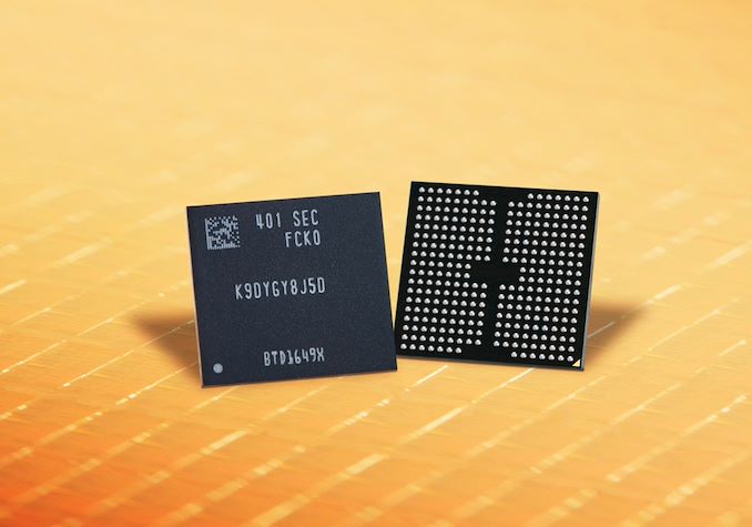
Samsung Electronics has started mass production of its 9th generation of V-NAND memory. The first dies based on their latest NAND tech come in a 1 Tb capacity using a triple-level cell (TLC) architecture, with data transfer rates as high as 3.2 GT/s. The new 3D TLC NAND memory will initially be used to build high-capacity and high-performance SSDs, which will help to solidify Samsung's position in the storage market.
Diving right in, Samsung is conspicuously avoiding to list the number of layers in their latest generation NAND, which is the principle driving factor in increasing capacity generation-on-generation. The company's current 8th gen V-NAND is 236 layers – similar to its major competitors – and word on the street is that 9th gen V-NAND ups that to 290 layers, though this remains to be confirmed.
Regardless, Samsung says that its 9th generation V-NAND memory boasts an approximate 50% improvement in bit density over its 8th generation predecessor. Driving this gains, the company cites the miniaturization of the cell size, as well as the integration of enhanced memory cell technologies that reduce interference and extend the lifespan of the cells. With their latest NAND technology, Samsung has also been able to eliminate dummy channel holes, thus reducing the planar area of the memory cells.
Interestingly, today's announcement also marks the first time that Samsung has publicly confirmed their use of string stacking in their NAND, referring to it as their "double-stack structure." The company is widely believed to have been using sting stacking back in their 8th generation NAND as well, however this was never confirmed by the company. Regardless, the use of string stacking is only going to increase from here, as vendors look to keep adding layers to their NAND dies, while manufacturing variability and channel hole tolerances make it difficult to produce more than 150-200 layers in a single stack.
| Samsung TLC V- NAND Flash Memory | ||
| 9th Gen V-NAND | 8th Gen V-NAND | |
| Layers | 290? | 236 |
| Decks | 2 (x145) | 2 (x118) |
| Die Capacity | 1 Tbit | 1 Tbit |
| Die Size (mm2) | ?mm2 | ?mm2 |
| Density (Gbit/mm2) | ? | ? |
| I/O Speed | 3.2 GT/s (Toggle 5.1) |
2.4 GT/s (Toggle 5.0) |
| Planes | 6? | 4 |
| CuA / PuC | Yes | Yes |
Speaking of channel holes, another key technological enhancement in the 9th gen V-NAND is Samsung's advanced 'channel hole etching' technology. This process improves manufacturing productivity by enabling the simultaneous creation of electron pathways within a double-stack structure. This method is crucial as it enables efficient drilling through more layers, which is increasingly important as cell layers are added.
The latest V-NAND also features the introduction of a faster NAND flash interface, Toggle DDR 5.1, which boosts peak data transfer rates by 33% to 3.2 GT/s, or almost 400MB/sec for a single die. Additionally, 9th gen V-NAND's power consumption has been reduced by 10%, according to Samsung. Though Samsung doesn't state under what conditions – presumably, this is at iso-frequency rather than max frequency.
Samsung's launch of 1Tb TLC V-NAND is set to be followed by the release of a quad-level cell (QLC) model later this year.
"We are excited to deliver the industry’s first 9th-gen V-NAND which will bring future applications leaps forward," said SungHoi Hur, Head of Flash Product & Technology of the Memory Business at Samsung Electronics. "In order to address the evolving needs for NAND flash solutions, Samsung has pushed the boundaries in cell architecture and operational scheme for our next-generation product. Through our latest V-NAND, Samsung will continue to set the trend for the high-performance, high-density solid-state drive (SSD) market that meets the needs for the coming AI generation."


