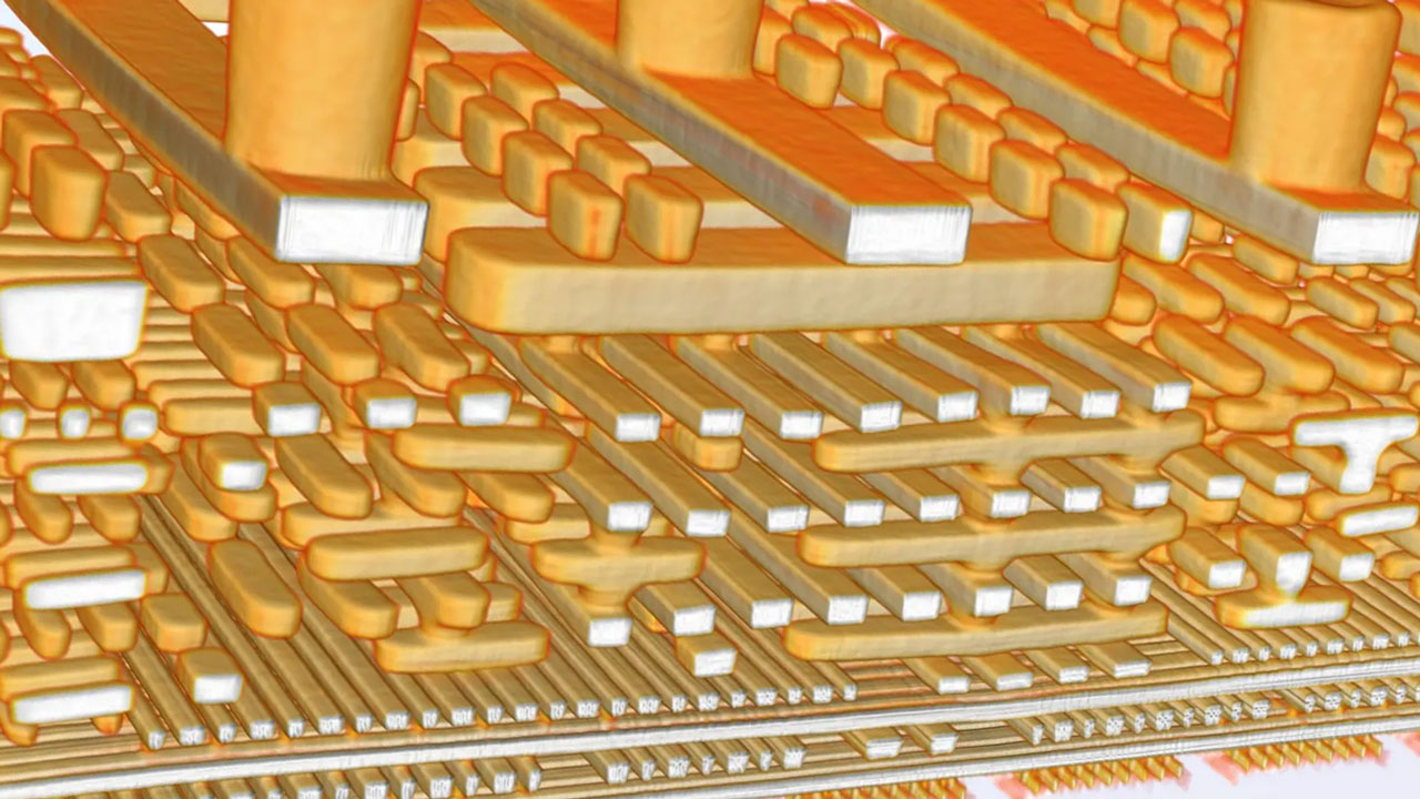
A team of scientists split between the Paul Scherrer Institute in Switzerland, the University of Southern California, and ETH Zürich were behind the vastly improved imaging technique dubbed PyXL, reports IEEE Spectrum. Initially, PyXL could resolve details as small as 19nm. Still, its fidelity has been tuned via burst ptychography to eliminate jitter, and now the system can have a resolution of 4nm.
Researchers have detailed a new X-ray technique that can see inside computer chips to reveal crisp and clear 3D images. To reveal the inside of a computer chip for analysis, engineers previously had to leverage destructive methods like slicing or grinding through layers of material before investigating with microscopy. Thus, the new non-destructive ptychographic X-ray laminography (PyXL) technology and its clear 3D images could greatly benefit the semiconductor industry.
Baohua Niu, a principal engineer at the Intel Foundry in Hillsboro, Oregon, provided some industry perspective on PyXL for the IEEE report. Niu said that before PyXL, engineers would have to use a mix of methods to try and narrow down the potential problem areas of a chip for further investigation. Once the area of interest was determined, the chip could then be sliced (destructively, obviously) across the selected spot for surface imaging with a transmission electron microscope (TEM). It is not an ideal workflow, with its hit-and-miss chip destruction.
Niu admits that the best PyXL resolution is four or five times lower than a TEM image. However, the much deeper 3D images (up to 5 micrometers) of PyXL versus the 10 to 30 nanometer depth visible via a TEM can be telling. Thus, PyXL should be much easier and faster at pinpointing chip issues, said Niu. Efficient design feedback is critical to engineers. “Here’s what you designed for; here’s what actually was made given your design,” notes Niu regarding the validation cycle.
The report on the new PyXL x-ray imaging also highlights that the researchers used PyXL to image AMD Ryzen processors built using TSMC’s 7nm process node. The resolution of the latest 3D x-ray tech is good enough to see the structure and features of Ryzen’s FinFET transistors, including details like the precise placement of transistors and the interconnects. Moreover, a 3D view will become an increasingly valuable asset as chips gain more and more 3D features as part of their architecture and packaging.
Interestingly, inconsistencies across chips are easy to see using PyXL. “You can figure out how good the engineering is and the manufacturing, explained the University of Southern California’s Tony Levi. “You can see the quality in one chip, the slipshod in another.” It seems that PyXL can see variances that precipitate the silicon lottery.


