
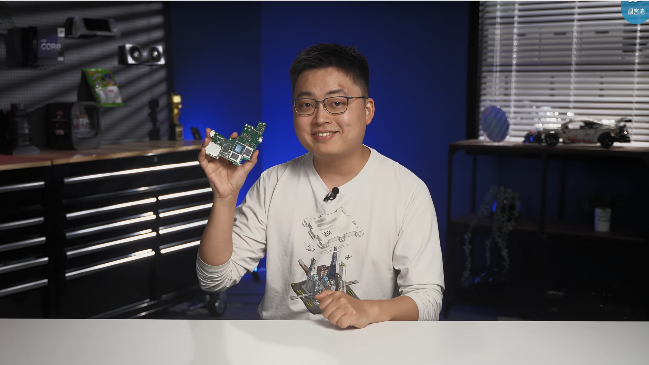
While we still have a month before the Nintendo Switch 2 makes its official debut, hardware sleuth Geekerwan managed to obtain an engineering board for the device. This allowed him to put the onboard Tegra T239 SoC under a FIB-SEM (Focused Ion Beam Scanning Electron Microscope) to examine the chip's internals, allowing for precise layer-by-layer analysis of the structure, revealing important details such as the core layout and process node.
Given Nintendo's strict legal stance and letigous precedents, it's quite amazing how Geekerwan managed to get ahold of the board, proceeded to dissect the SoC, and spilled all the juicy details on YouTube. Apparently, the board was acquired by hardware analyst Kurnal from Xianyu (Taobao's version of eBay) and then passed on to Geekerwan. Either way, this analysis answers many questions, as Nintendo has yet to officially disclose many SoC details.