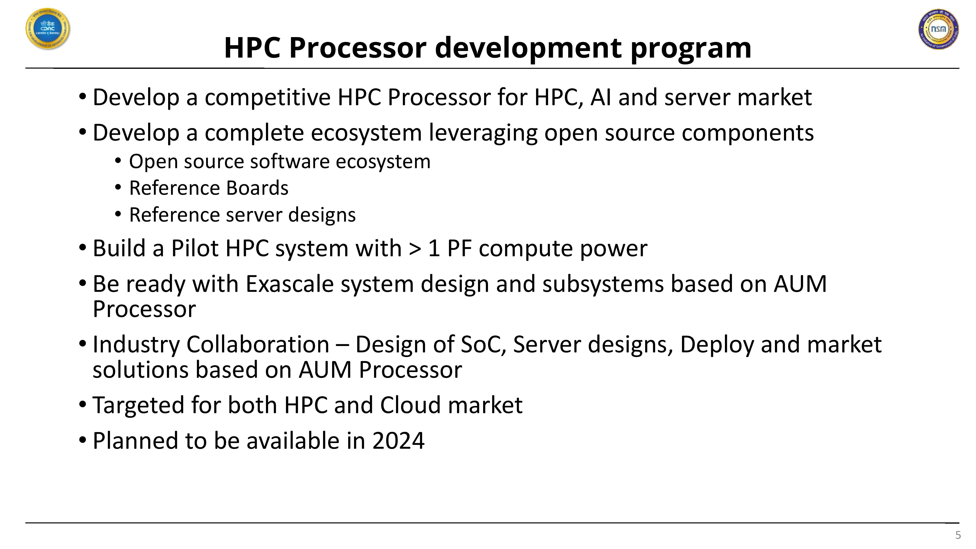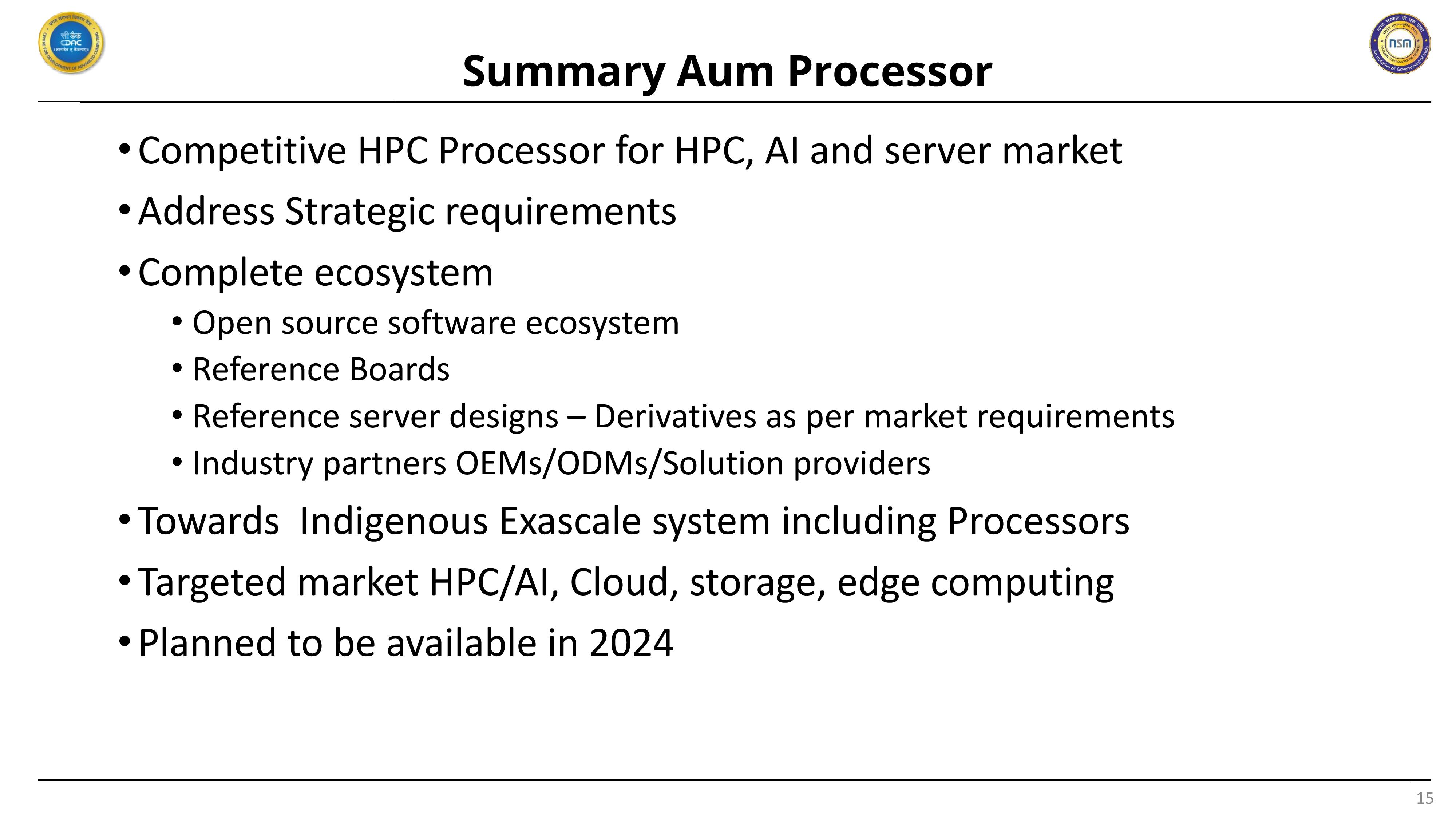
India's Center for Development of Advanced Computing (C-DAC) this week announced[PDF] the country's first self-designed High Performance Computing (HPC) CPU. Named Aum, India's first chip is a chiplet design that can scale up to 96 cores and is based on Arm's v8.4 "Zeus" Neoverse V1 designs (the same ones AWS uses in its Graviton3), and is expected to hit the market as early as 2024 on TSMC's 5 nm process.
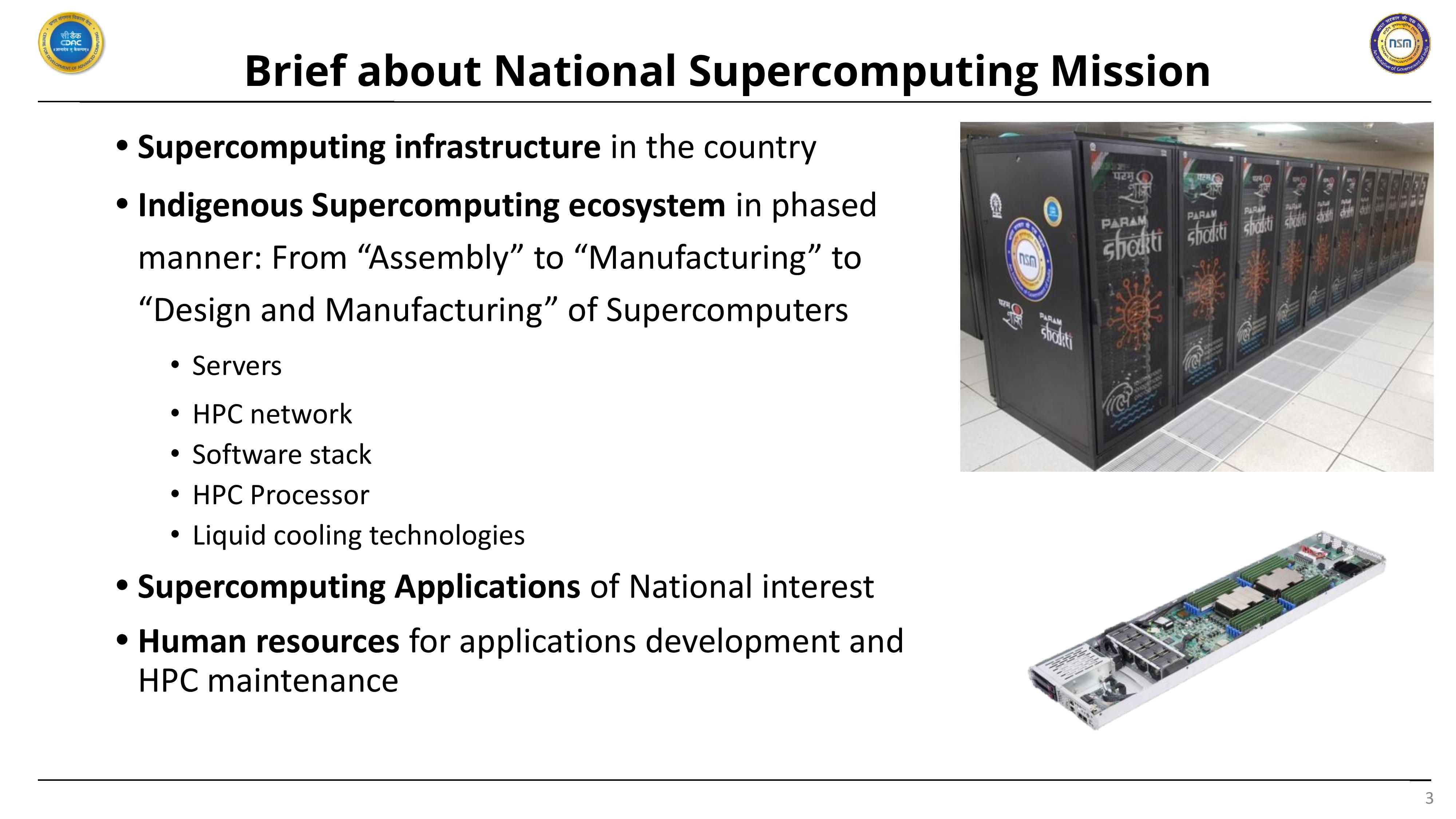
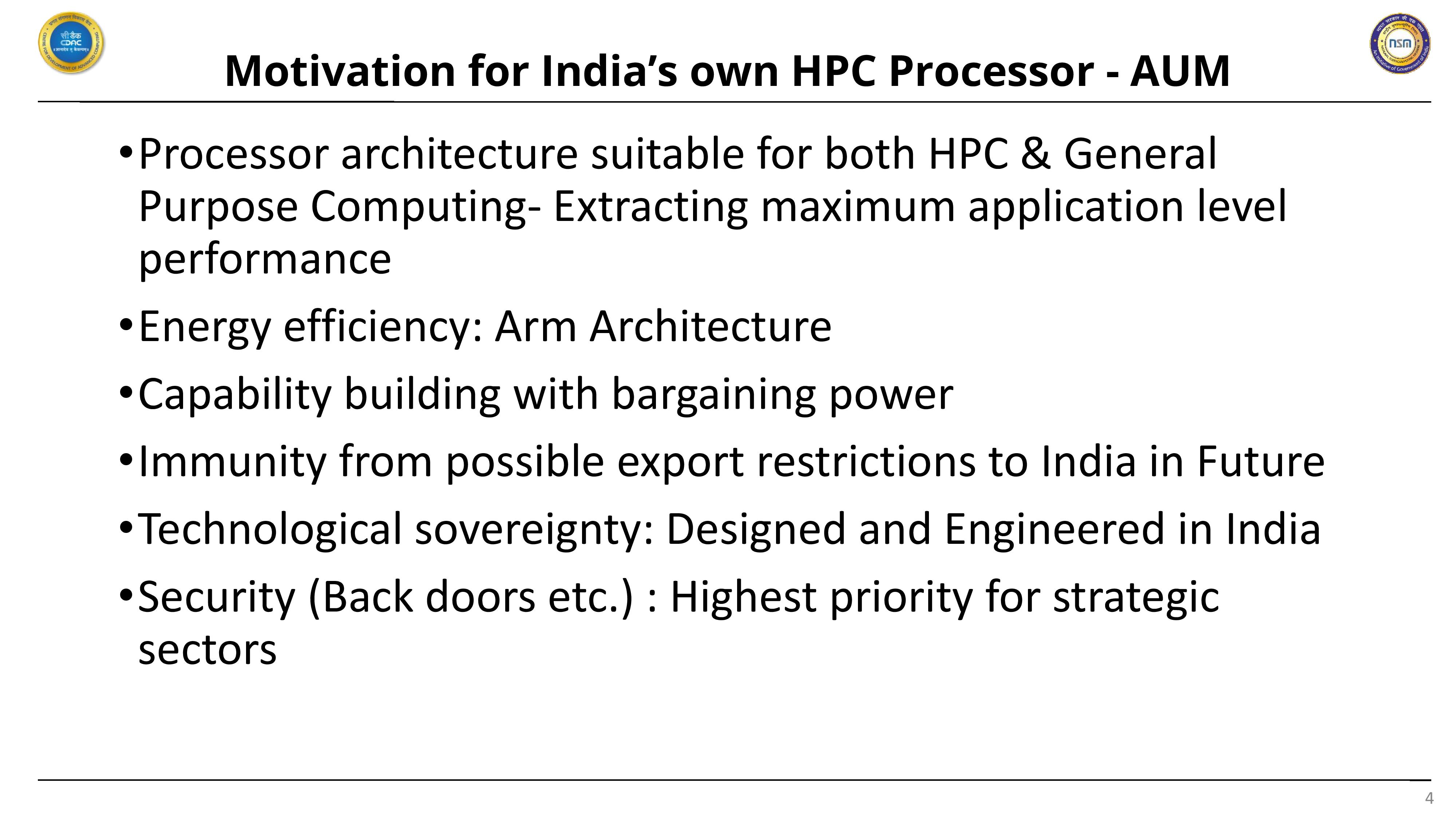
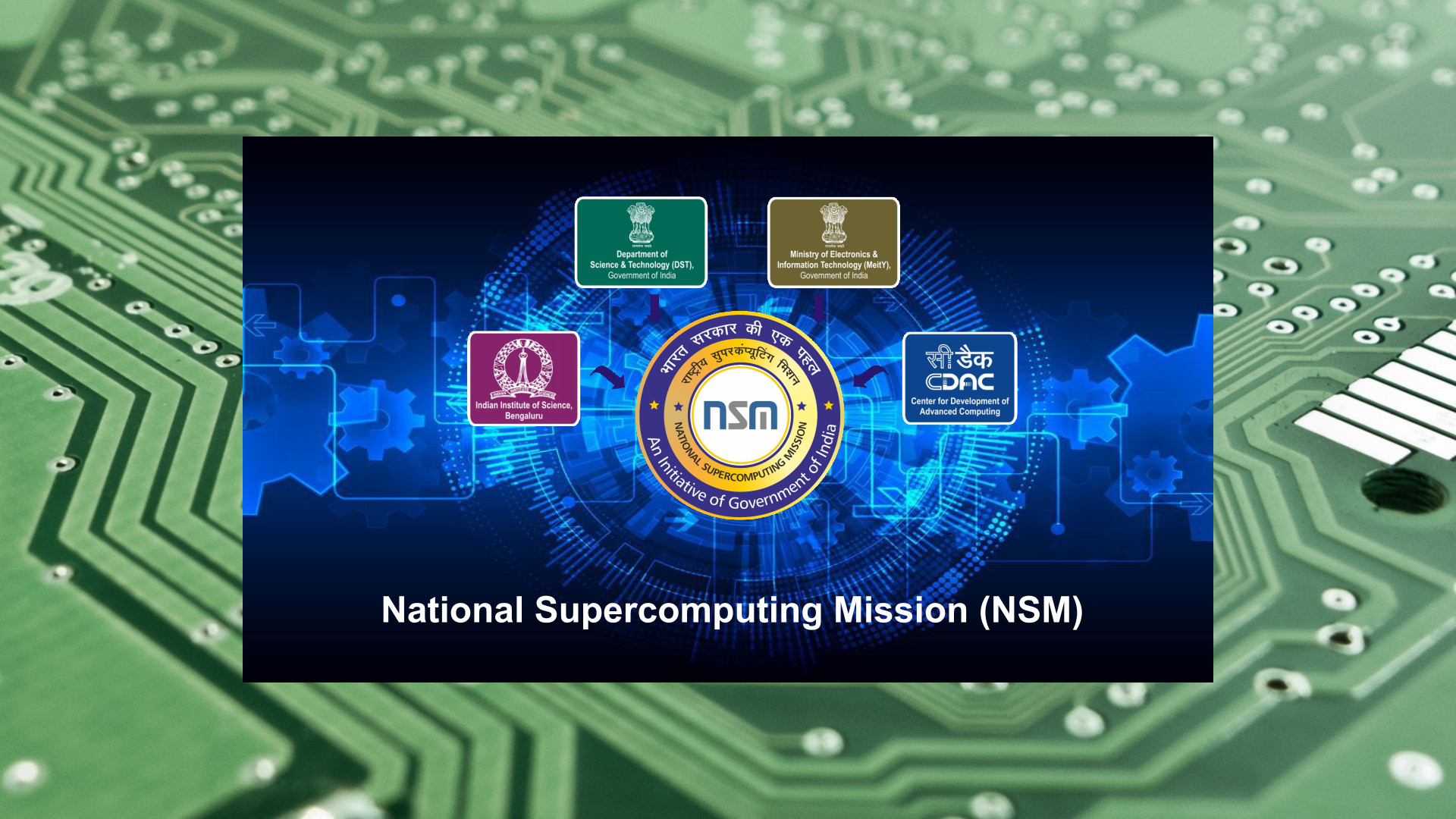
Aum was developed as part of its National Supercomputing Mission, a program that aims to reduce India's exposure to possible export restrictions. To that end, the aim is to deploy a nationally-developed processor architecture. Perhaps alarmingly for both Intel and AMD, however, the aim is for Aum to be useable in both high performance computing scenarios as well as personal computing chips. And where Aum exists, the market is smaller.
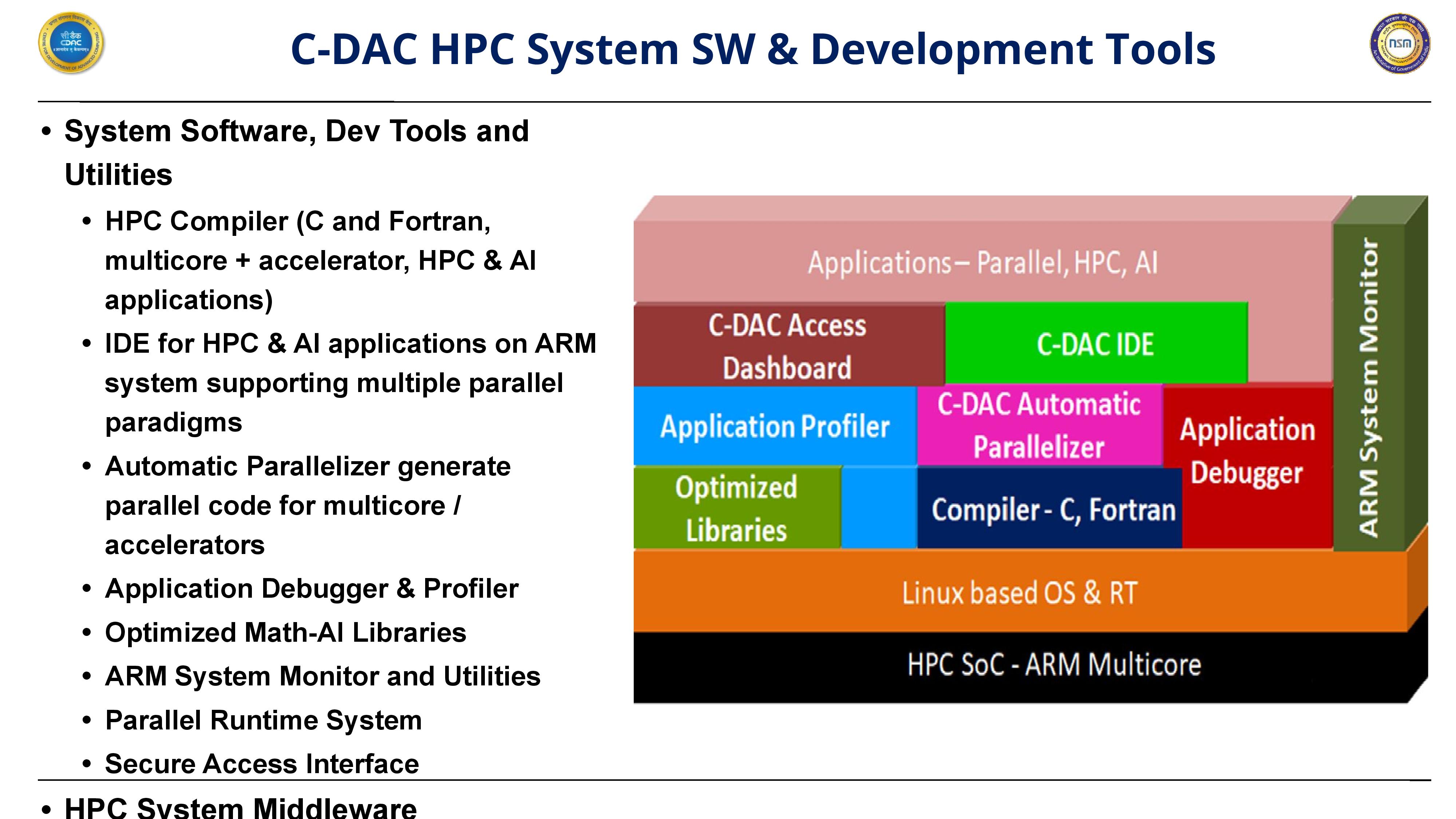
The reasoning is simple: if India has the capability to design chips (whether that means mix and matching pieces out of Arm's open-handed portfolio or guiding specific implementations for the final, manufacturable design), possible technological export restrictions could a little less. At the same time, the National Computing Mission also aims to improve security against eventual backdoors; a neutral design provider such as Arm naturally fits into those concerns. And while controlling the design process itself doesn't get it all the way there (not when backdoors can be applied on the factory floor by willing and capable adversaries), it's a strong start. The planned usage of open source software to prop up a specialized software ecosystem also paints a more diversified software future, so hardware isn't the only segment that's likely to fragment, given enough time.

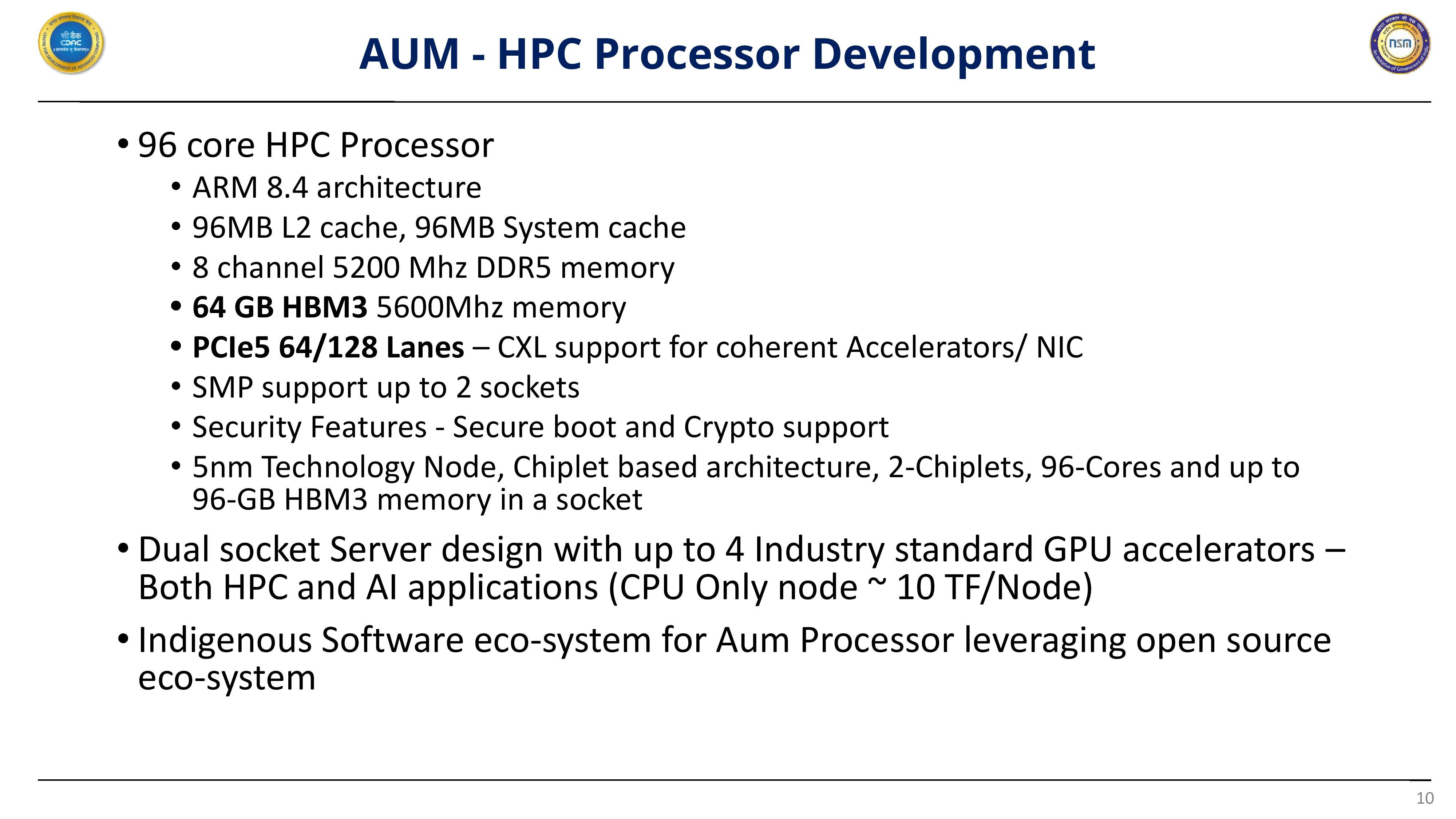
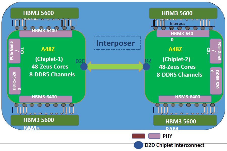
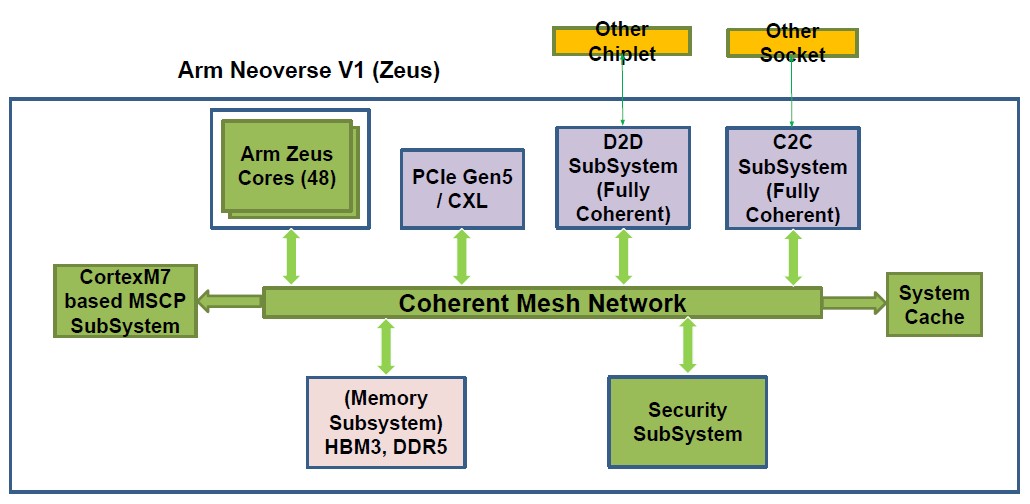
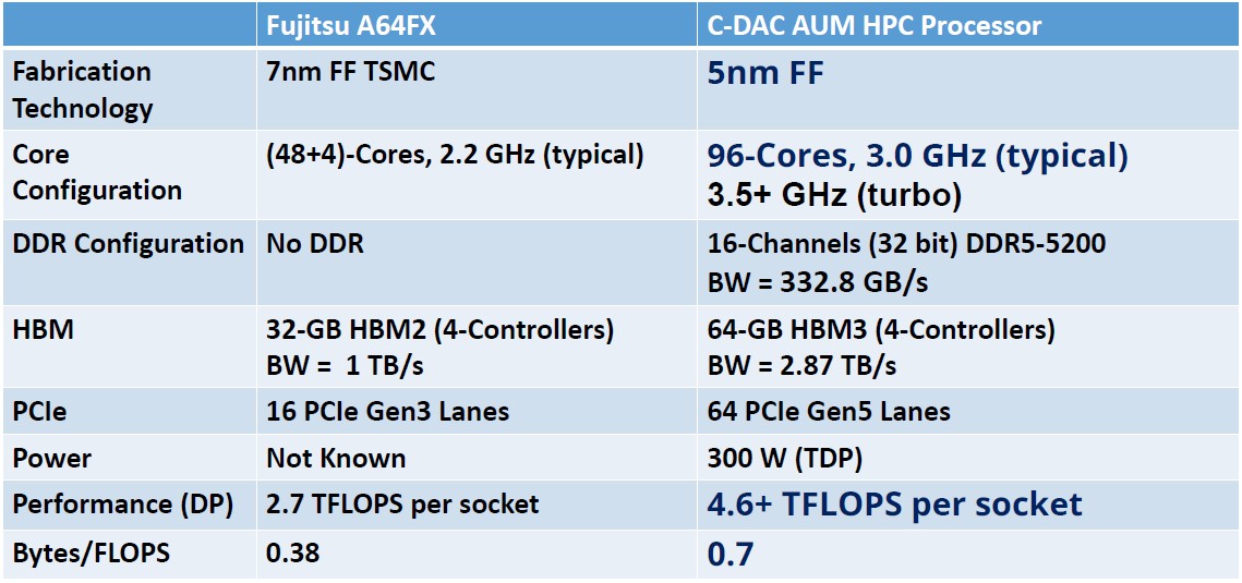
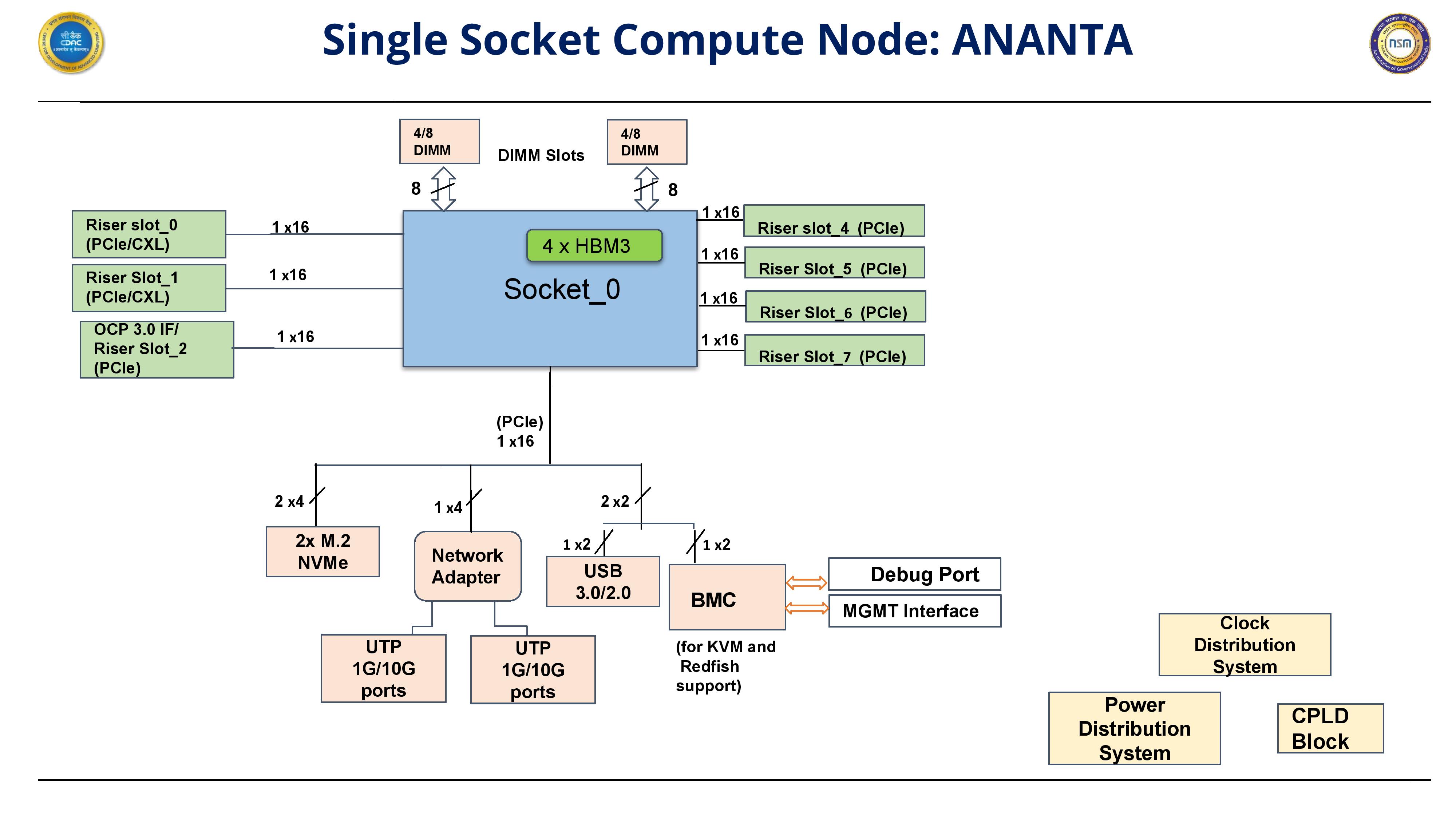
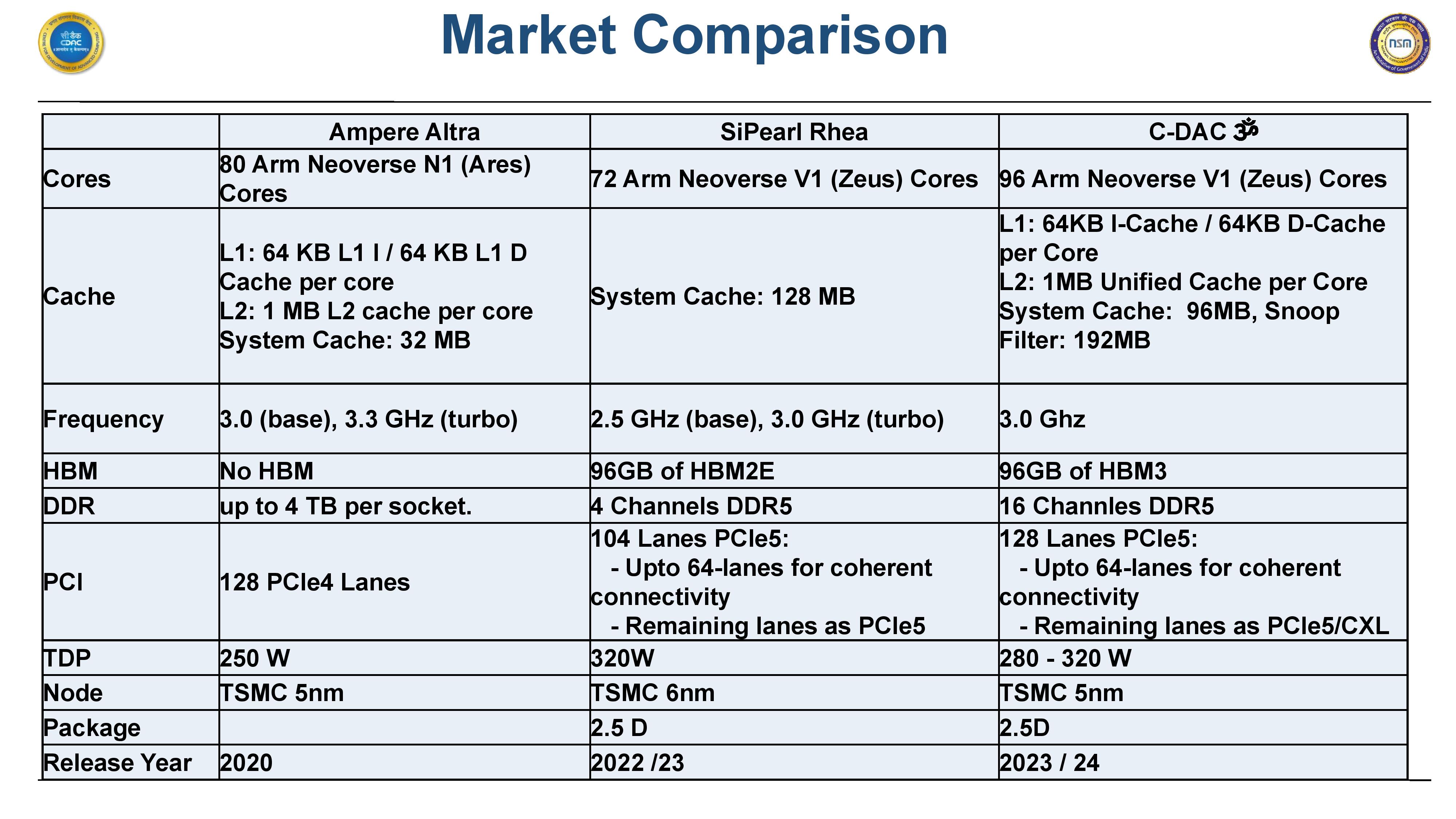
The A48Z chiplets at the heart of the 96-core Aum chip each feature 48 Arm Zeus cores (3 GHz base, 3.5 GHz Turbo), supported by 96 MB of immediate-access L2 cache and another 96 MB cache layer buffering the cores and the additional system memory. All in all, each Aum package supports up to 16 DDR5 memory channels (at 5200 MHz, delivering 332.8 GB/s of bandwidth) and 64 GB of HBM3 memory (6.4 GHz stock, geared down to 5.6 GHz at initial release for a staggering 2.87 TB/s). Additional byte throughput is added by the 128 PCIe Gen 5 lanes, 64 of which enable additional accelerators (such as GPU or FPGA accelerators).

The remaining 64 are likely routed for the chip's internal communications fabric, a coherent mesh network of NUMA-style, fully memory coherent links based on the CCIX protocol. This linked is used by two Aum sockets to communicate, and it takes a design page or two from AMD's Infinity Fabric.

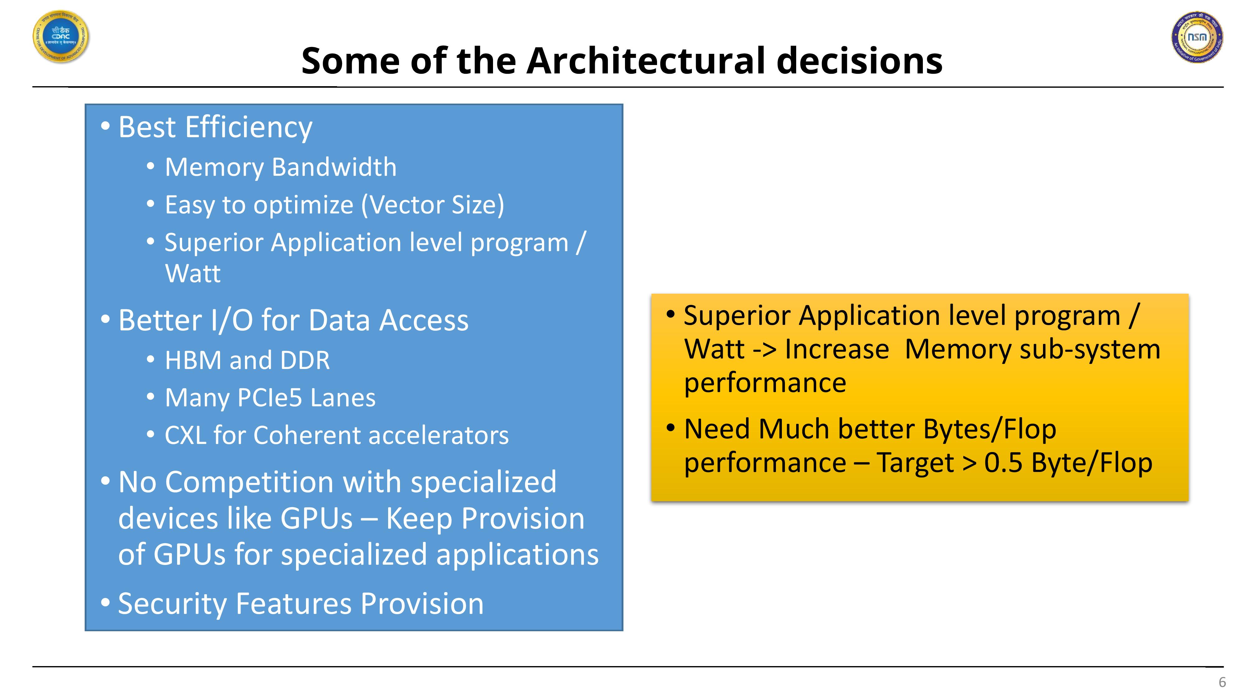
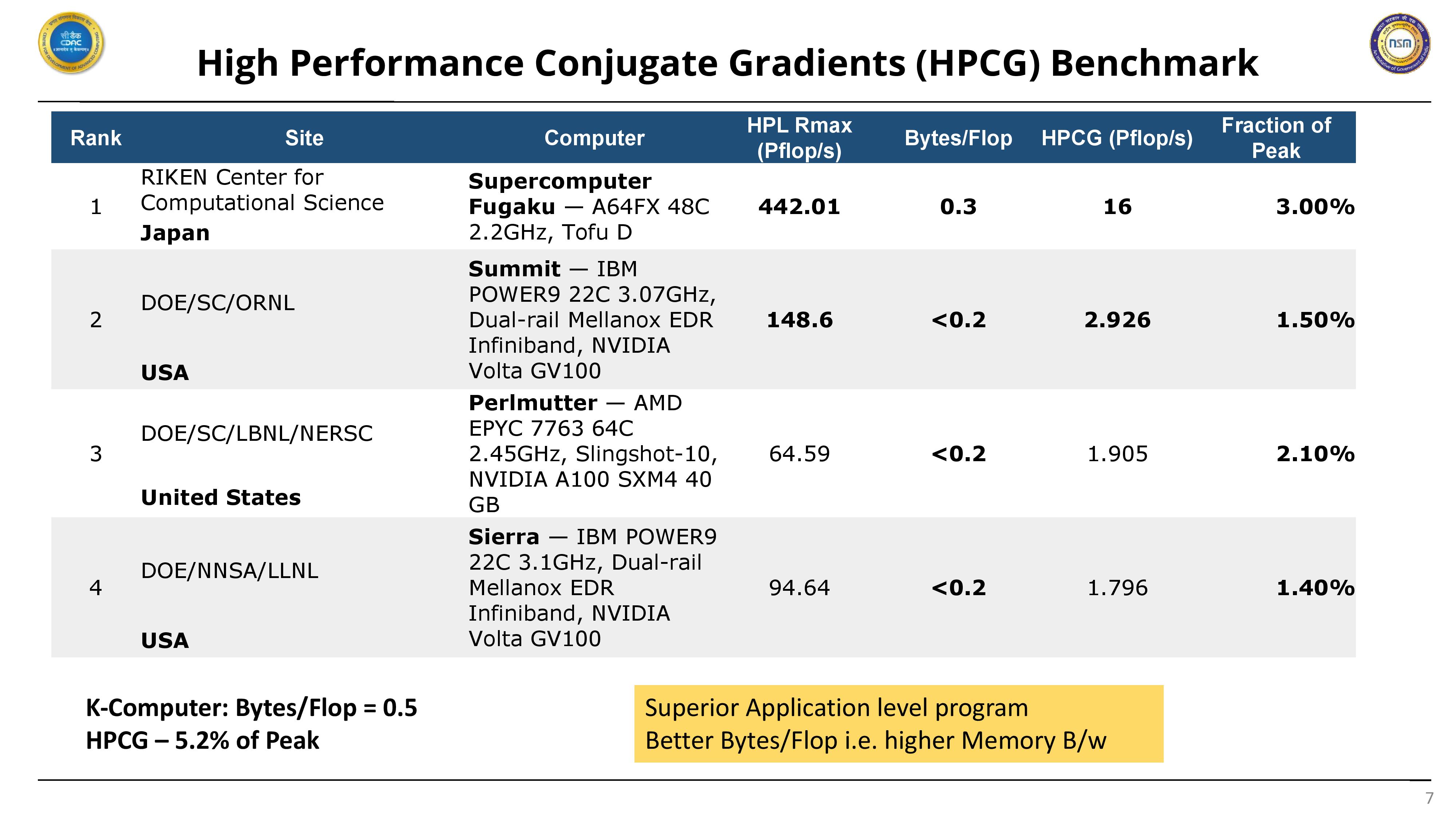
According to the documentation, Aum's design primarily aims to increase the amount of memory bandwidth available per flop of computing power (the byte/flop ratio), which has been found to be a highly limiting factor in performance scaling for HPC computation. Too many cars (floating operations per second) on too few lanes (memory throughput) can only end one way. The result is that Aum and its Arm architecture target performance at 4.6 teraflops per socket and 3 TB/sec of aggregate memory bandwidth. That'll give it a byte/flop ratio of 0.7, much higher than the 0.38 hit by the world's fastest Arm supercomputer, Japan's Fugaku, and decisively beating USA's IBM and Nvidia-based Summit (<0.2 bytes/flop). At an expected 300 W TDP, however, it seems energy efficiency actually declined compared to Fugaku's A64FX Arm cores.

If everything goes to plan, India's Aum Arm CPU will be a strong entry into the supercomputing field. Crucially, it'll be a homegrown one - even if not dramatically so, at least in its first iterations. Much work was clearly put into advancing the memory subsystem as a whole, and in general, memory is easier and more available to source than the TSMC 5 nm chips Aum will be made of. Customizing the CPU core itself could be C-DAC's next step, preparing the way for India and adding momentum to the "chip nationalization" process in other countries. China too has had an interest in Arm, by the way; but that is an entirely different story.
This broader push for a more varied chip ecosystem is part of the reason why Intel decided to reinvest into its Foundry client-chip business, a move its rival AMD did years ago (while in the midst of one of its most difficult corporate restructures ever). And it's yet another victory for the Arm ecosystem compared to its sometimes troubled x86 alternative, which in itself also punishes some harder than others.
It's also, perhaps, a sign of things to come when it comes to shipping volumes for semiconductor manufacturers: ever more entities are pitching and receiving their designs from the waters of TSMC, yet there are only so many wafers for all the takers - and crumbs from volume fights are already littering the floor.
The full slide deck follows.
