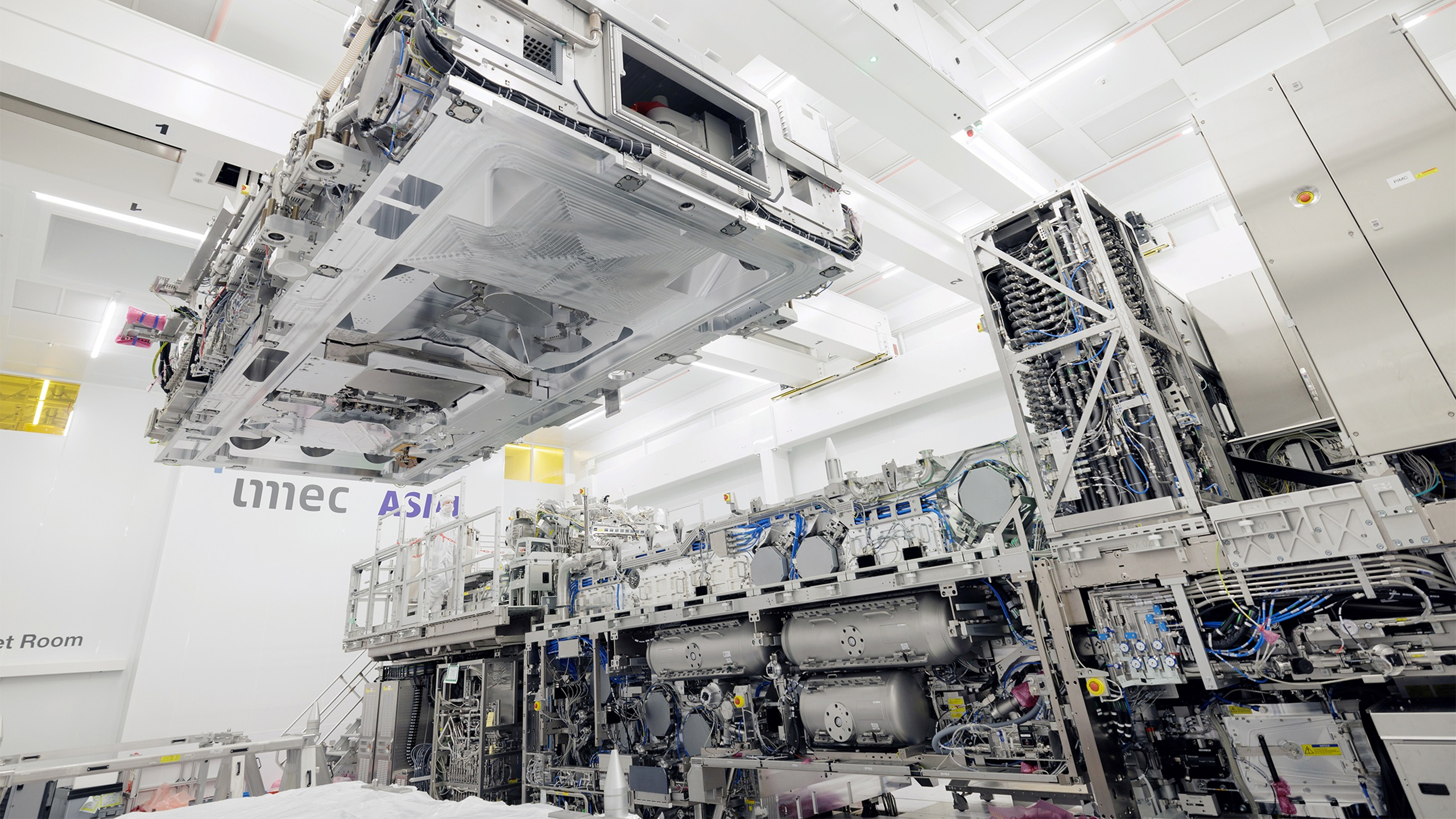
Imec and ASML announced on Wednesday that they had made the industry’s logic and DRAM structures using ASML'sASML’sroduction Twinscan EXE:5000 EUV lithography tool with a 0.55 numerical aperture, also known as a high-NA litho system. The successful demonstration of high-resolution patterning with the 0.55NA EUV scanner marks an essential milestone in microelectronics production.
Imec achieved the patterning of random logic structures with 9.5nm dense metal lines (compared to a 13nm resolution in the case of currently used Low-NA tools), which corresponds to a 19nm pitch and a sub 20nm tip-to-tip dimensions, which is good enough to build logic on a 1.4nm-class process technology using a single High-NA exposure. Additionally, Imec successfully created random vias with a 30nm center-to-center distance, showcasing good pattern fidelity and critical dimension uniformity. Furthermore, 2D features were patterned at a 22nm pitch, which is good enough for a 3nm-class fabrication process.