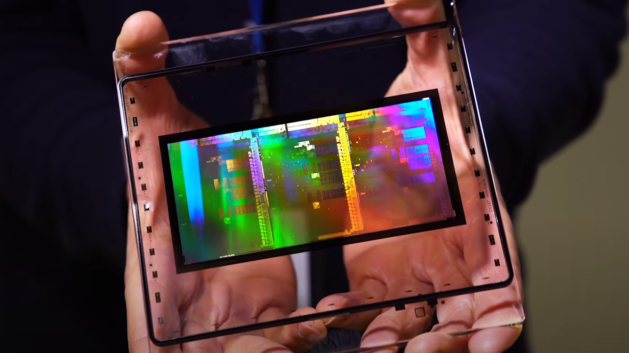
Corning is primarily known for its ruggedized glasses for smartphones and is barely known in the semiconductor industry. Yet, its contribution to the production of chips using leading-edge technologies is rather huge. To that end, the company is eligible to get money from the CHIPS and Science Act fund. This week, Corning and the U.S. Department of Commerce inked a preliminary agreement under which Corning is set to get $32 million.
Corning makes various glass materials to build photomasks, such as high-purity fused silica, ultra-low expansion (ULE), and extreme ULE glass. A major advantage of ULE and Extreme ULE materials is their exceptionally low thermal expansion to ensure maximum consistency in harsh EUV environments (which are getting harsher as EUV tools gain more powerful light sources to increase performance) and exceptional uniformity to reduce photomask ‘waviness’ to minimize circuit variability (i.e., lower performance and power variability).
Corning’s ULE glass is used to make photomasks for DUV and EUV lithography, whereas Extreme ULE material is projected for next-generation High-NA EUV lithography.
Ensuring that companies in America that use advanced DUV, Low-NA EUV, and High-NA EUV tools have access to materials used to make photomasks is crucial for the whole industry in general and companies like Intel, GlobalFoundries, TSMC, Texas Instruments, and Samsung Foundry.
Corning’s $32 million funding will support the expansion of its manufacturing facility in Canton, New York, to increase the production of specialized materials like high-purity fused silica (HPFS) and Extreme ULE glass. This project will add 130 manufacturing jobs and over 175 construction jobs.
“Corning is proud to be an industry leader of specialty glass and precision optical lenses for the semiconductor industry, and our Canton facility plays a vital role in the nation’s mission to strengthen the domestic semiconductor supply chain,” said Corning Incorporated Chairman and CEO Wendell Weeks. “This proposed investment and the continued commitment in Canton will enable us to establish the next-generation manufacturing capabilities needed to produce vital materials for lithography tools that will develop the world’s most complex microchips, strengthening our commitment to advancing semiconductor technology and job creation in the United States.”


