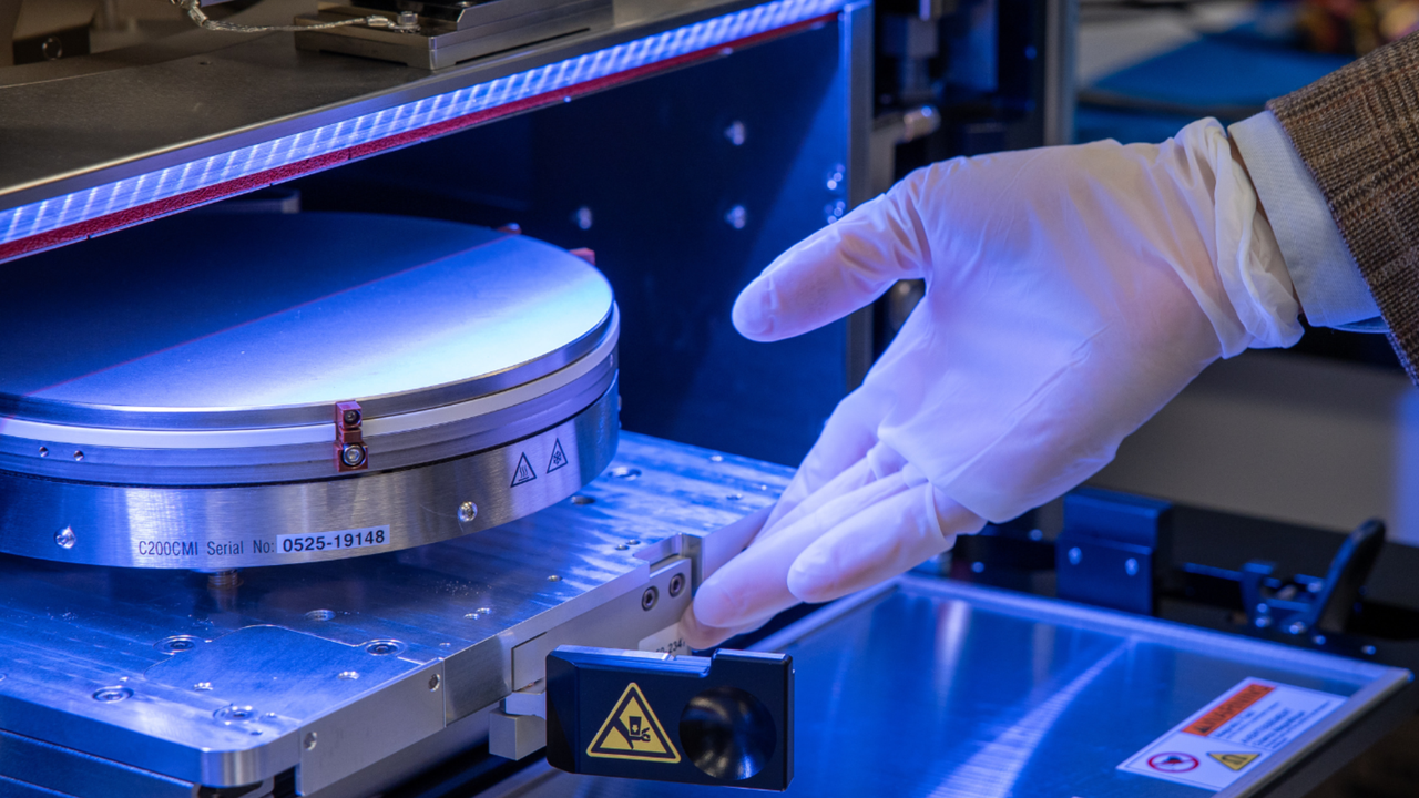
A collaborative research team has demonstrated what it says is the first monolithic 3D integrated circuit manufactured at a commercial U.S. foundry, reporting substantial performance gains over conventional flat chip designs. The prototype was developed by engineers from Stanford, Carnegie Mellon, the University of Pennsylvania, and MIT, and fabricated in partnership with SkyWater Technology.
The chip departs from conventional two-dimensional layouts by stacking memory and logic directly on top of one another in a single, continuous process. Instead of assembling multiple finished dies into a package, the researchers built each device layer sequentially on the same wafer using a low-temperature process designed not to damage underlying circuitry, resulting in a dense network of vertical interconnects that shortens data paths between memory cells and compute units.