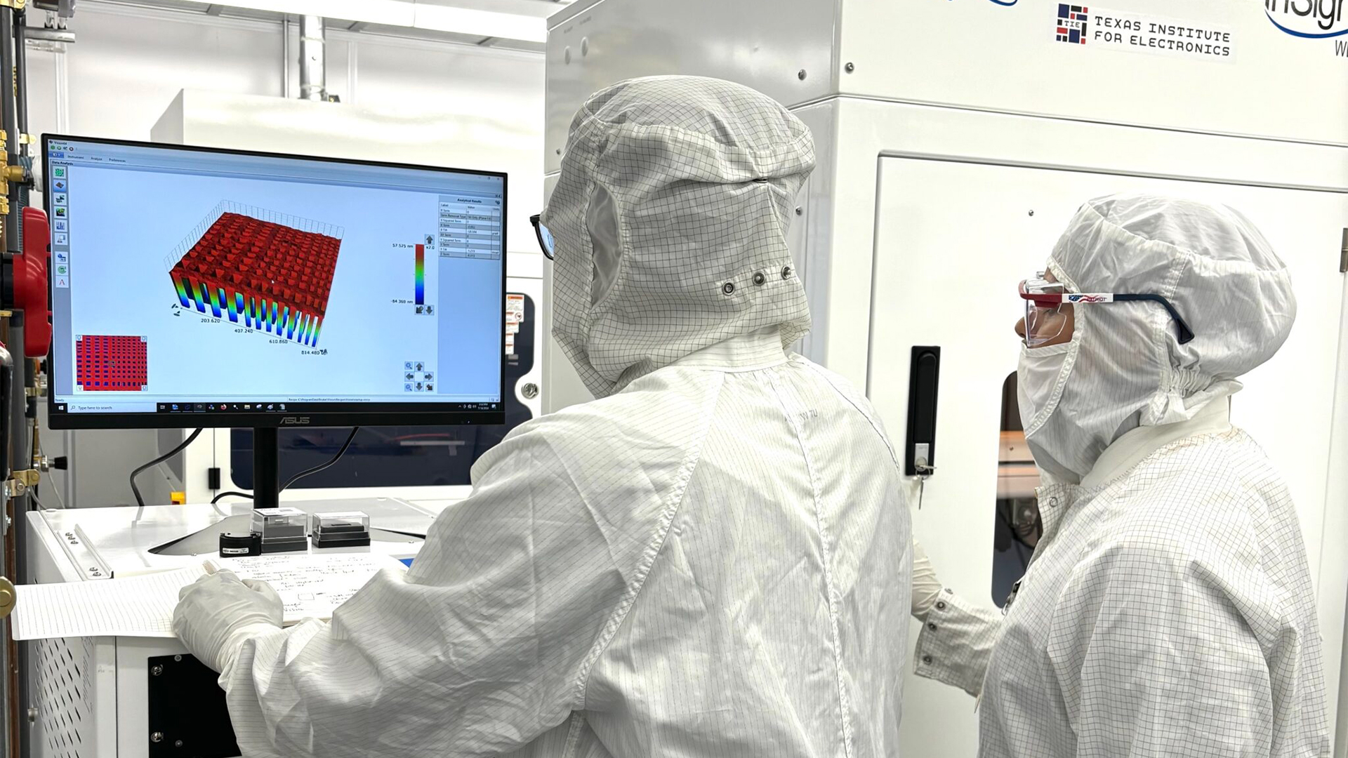
DARPA has selected the Texas Institute for Electronics (TIE) at The University of Texas (UT) at Austin to develop 3D-integrated multi-chiplet advanced 'semiconductor microsystems' for the U.S. Department of Defense. This project involves creating a national R&D and prototyping facility to produce high-performance, energy-efficient, lightweight, and compact defense systems.
A $1.4 billion project
The project is part of DARPA's Next Generation Microelectronics Manufacturing (NGMM) program, which aims to design 3D packaging technologies and build appropriate facilities for military and civil use. The project involves a $1.4 billion investment, with DARPA contributing $840 million and the Texas Legislature pouring in another $552 million in TIE.
This funding will be used to modernize two UT fabrication facilities that are set to foster dual-use innovations in the 3DHI multi-chiplet integration for both the defense sector and the semiconductor industry. These facilities will be self-sustained and accessible to academia, industry (including startups), and government.
The program spans two phases, each lasting 2.5 years. In the first phase, TIE will focus on building the center's infrastructure and foundational capabilities. The second phase will involve creating 3D-integrated (3DHI) hardware prototypes crucial to the DoC and automating various processes. Additionally, TIE will collaborate with DARPA on other separately funded design challenges.
"By investing in leading-edge microelectronics manufacturing, we are helping secure this vulnerable supply chain, boosting our national security and global competitiveness, and driving innovation in critical technologies," said U.S. Sen. John Cornyn. "The next generation of high-performing semiconductors these resources will enable through DARPA's partnership with UT TIE will help not only bolster our defense but also pave the way for the U.S. to reclaim its leadership role in this critical industry, and I look forward to seeing more Texas-led advancements in the years to come."
Military-grade 3D packaging
Modern military applications rely on several discreet chips, which usually complicates these systems and makes them more expensive. The reason why jets or unmanned aerial vehicles use many chips is simple: each chip is responsible for a certain application (e.g., radar is one high-power chip made using GaN, aiming assistance is a typical high-performance made on an enhanced bulk silicon fabrication process) and is produced using a process technology that is best fit for this particular workload. The new project will attempt to build multi-chiplet designs that integrate different logic into one package and make that package as small as possible. As a result, these system-in-packages (SiP) will enable smaller, lighter military devices.
While most of the process technologies offered by companies like Intel, GlobalFoundries, or TSMC (now that it is in the U.S.) are good enough for many uses, some aerospace and military applications demand more rigidity, which is why specialized process technologies will still be in use for at least a while. Still, Intel's 18A is going into some military applications, and this is just a start for the leading-edge nodes to enter this space.
When it comes to multi-chiplet packaging technologies, things are similar. Advanced packaging technologies must be aerospace and military-grade, and they do not look like 'off-the-shelf' methods from existing manufacturers that meet all of the U.S. DoC's needs. This is where DARPA's NGMM program, introduced in late 2023, comes in.
Summary
While sophisticated multi-chiplet processors will enhance U.S. national security and global military leadership, the labs and manufacturing capability in Texas developed as part of the project will be accessible to developers and producers of civil applications too, which means a potential boost to the scientific innovation and the industrial might of the USA.


