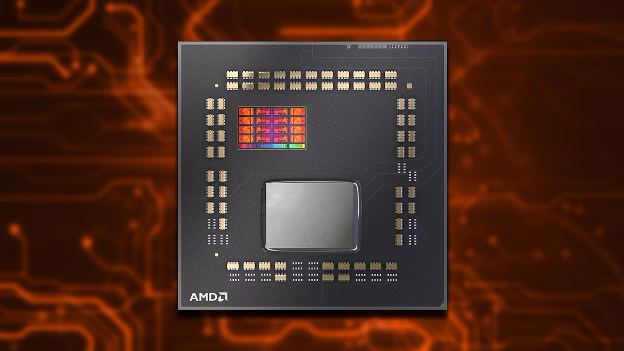
In two weeks, AMD will introduce its Ryzen 9000X3D chips, which will rival the best CPUs on the market. Hardware leaker HXL on X has clarified, to some extent, the architectural differences between the first and second generations and why AMD can achieve better thermals and higher clock speeds with Ryzen 9000X3D. It is claimed that AMD is reversing its 3D die-stacking structure, with the SRAM block now placed beneath the CCDs.
When AMD first launched its Ryzen 5000X3D chips, the concept was to stack a block of L3 cache atop the CCDs. A large issue with this model was heat dissipation due to using extra silicon over the CCDs for structural integrity. This thermal constraint also restricted AMD from bumping the clock speeds on these processors. However, that seems to be addressed with Ryzen 9000X3D, as the CCD reportedly sits atop the cache die. If true, AMD's new design will genuinely be an engineering marvel - from both architectural and packaging standpoints.