TSMC announced its leading-edge 1.6nm-class process technology today, a new A16 manufacturing process that will be the company's first Angstrom-class production node and promises to outperform its predecessor, N2P, by a significant margin. The technology's most important innovation will be its backside power delivery network (BSPDN).
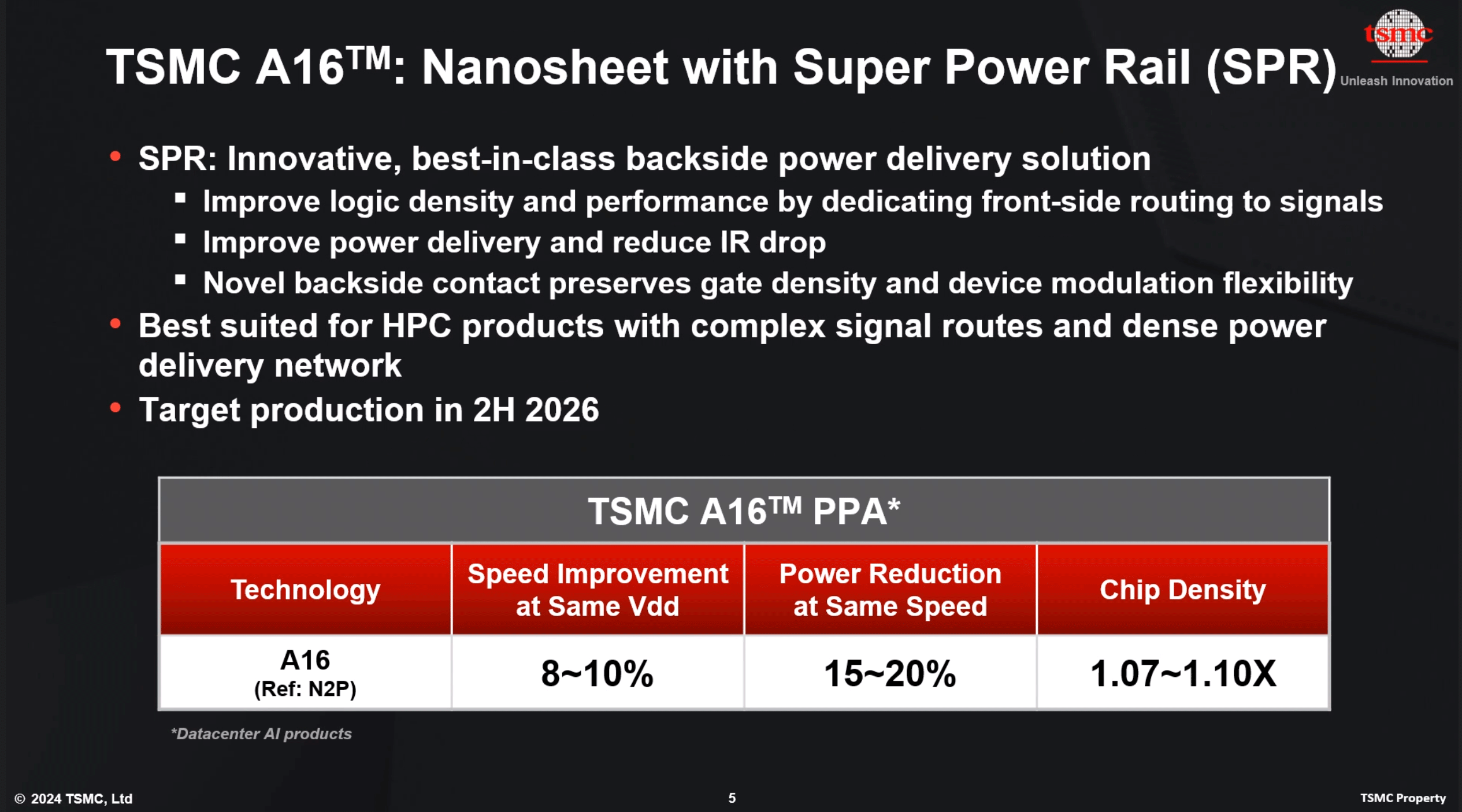
Just like TSMC's 2nm-class nodes (N2, N2P, and N2X), the company's 1.6nm-class fabrication process will rely on gate-all-around (GAA) nanosheet transistors, but unlike the current and next-generation nodes, this one uses backside power delivery dubbed Super Power Rail. Transistor and BSPDN innovations enable tangible performance and efficiency improvements compared to TSMC's N2P: the new node promises an up to 10% higher clock rate at the same voltage and a 15%–20% lower power consumption at the same frequency and complexity. In addition, the new technology could enable 7%–10% higher transistor density, depending on the actual design.

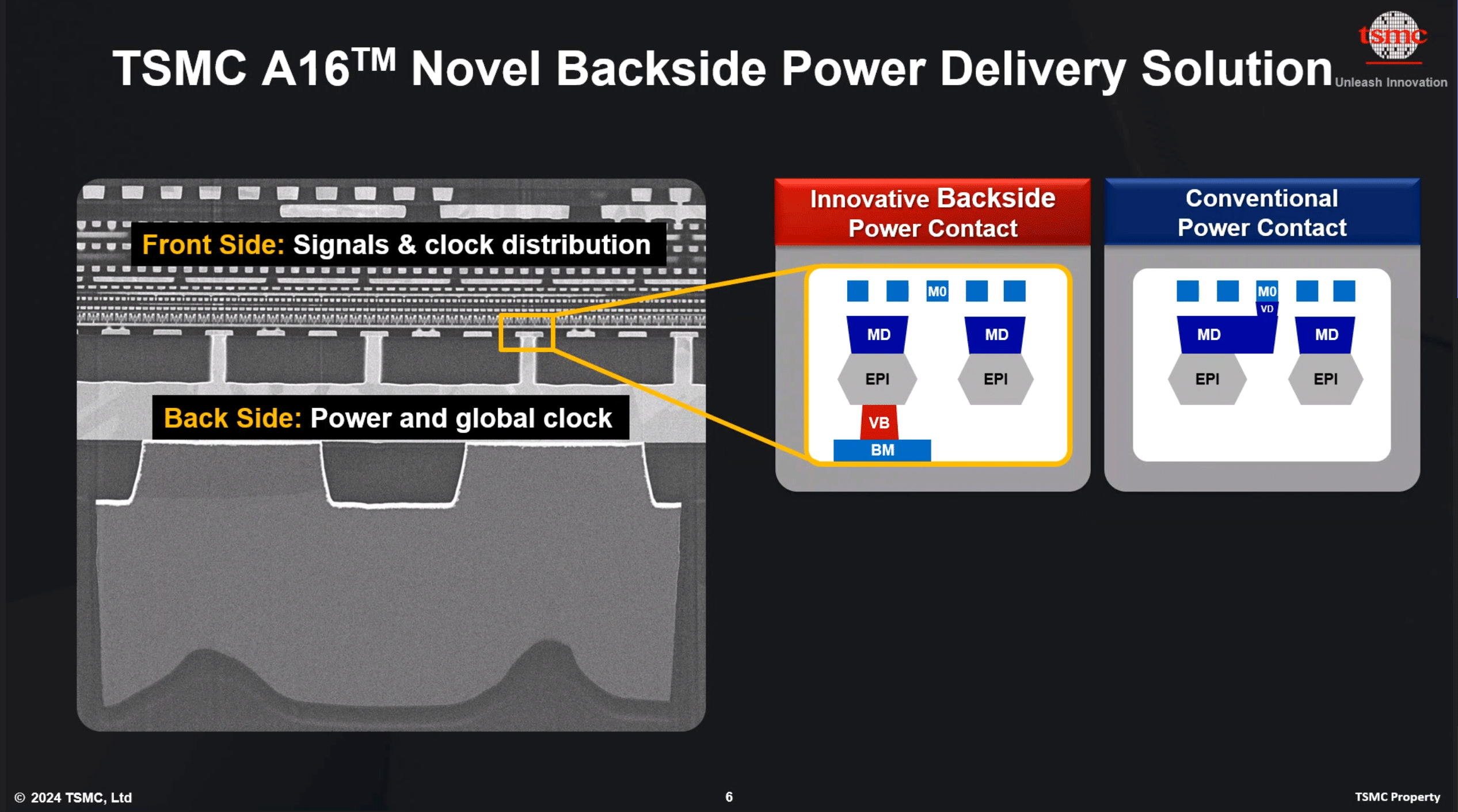
The most important innovation of TSMC's A16 process, which was unveiled at the company's North American Technology Symposium 2024, is the introduction of the Super Power Rail (SPR), a sophisticated backside power delivery network (BSPDN). This technology is tailored specifically for AI and HPC processors that tend to have both complex signal wiring and dense power delivery networks.
Backside power delivery will be implemented into many upcoming process technologies as it allows for an increase in transistor density and improved power delivery, which affects performance. Meanwhile, there are several ways to implement a BSPDN. TSMC's Super Power Rail plugs the backside power delivery network to each transistor's source and drain using a special contact that also reduces resistance to get the maximum performance and power efficiency possible. From a production perspective, this is one of the most complex BSPDN implementations and is more complex than Intel's Power Via.

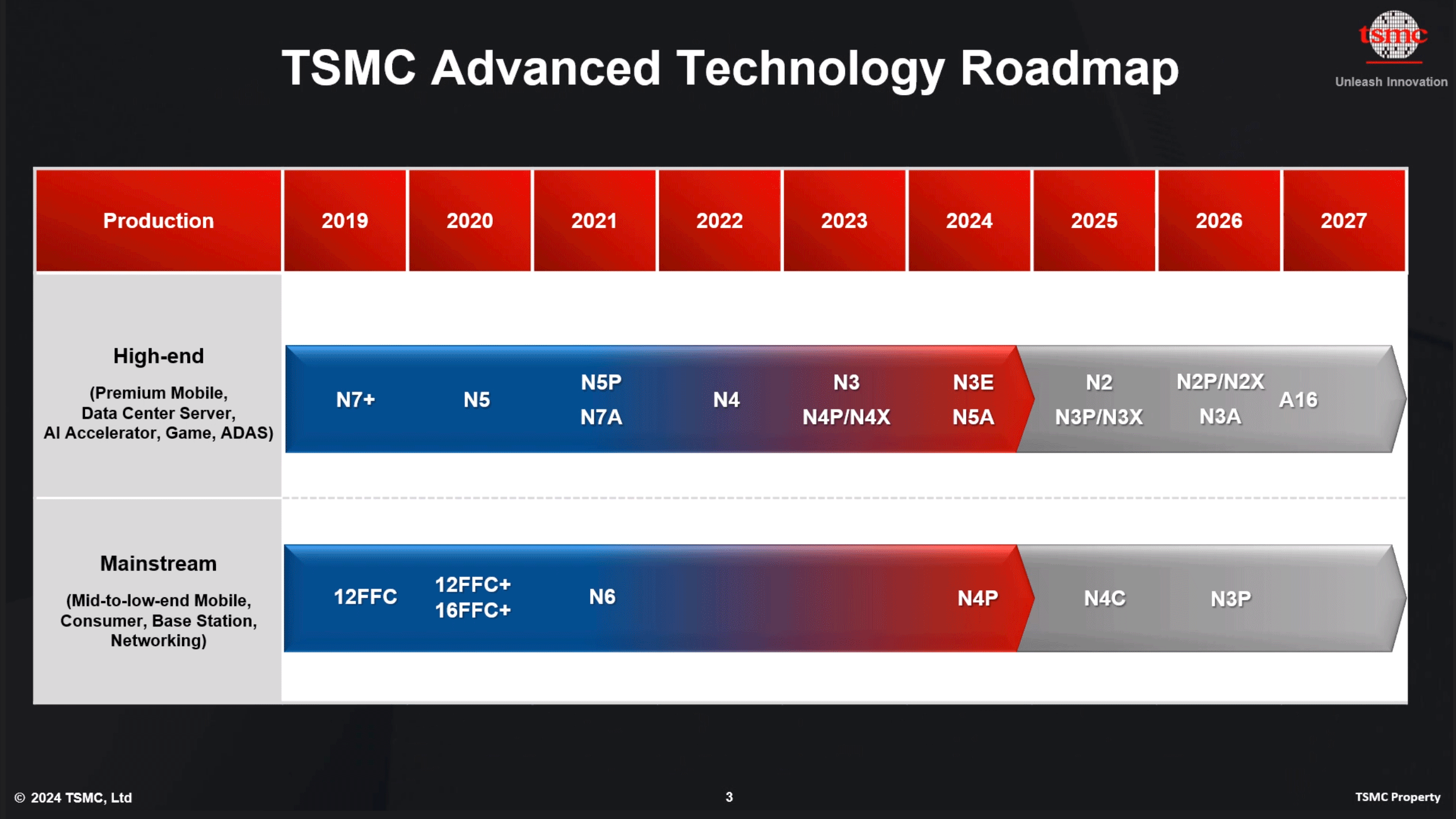
The choice of backside power rail implementation is perhaps why TSMC decided not to add this feature to its N2P and N2X process technologies, as it would make using the production nodes considerably more expensive. Meanwhile, by offering a 1.6nm-class node with GAA nanosheet transistors and SPR as well as 2nm-class nodes with GAAFETs only, the company will now have two distinct nodes that will not compete with each other directly but offer distinctive advantages for different customers.

The production timeline for A16 indicates that volume production of A16 will commence in the second half of 2026. Therefore, actual A16-made products will likely debut in 2027. This timeline positions A16 to potentially compete with Intel's 14A node, which will be the Intel's most advanced node at the time.


