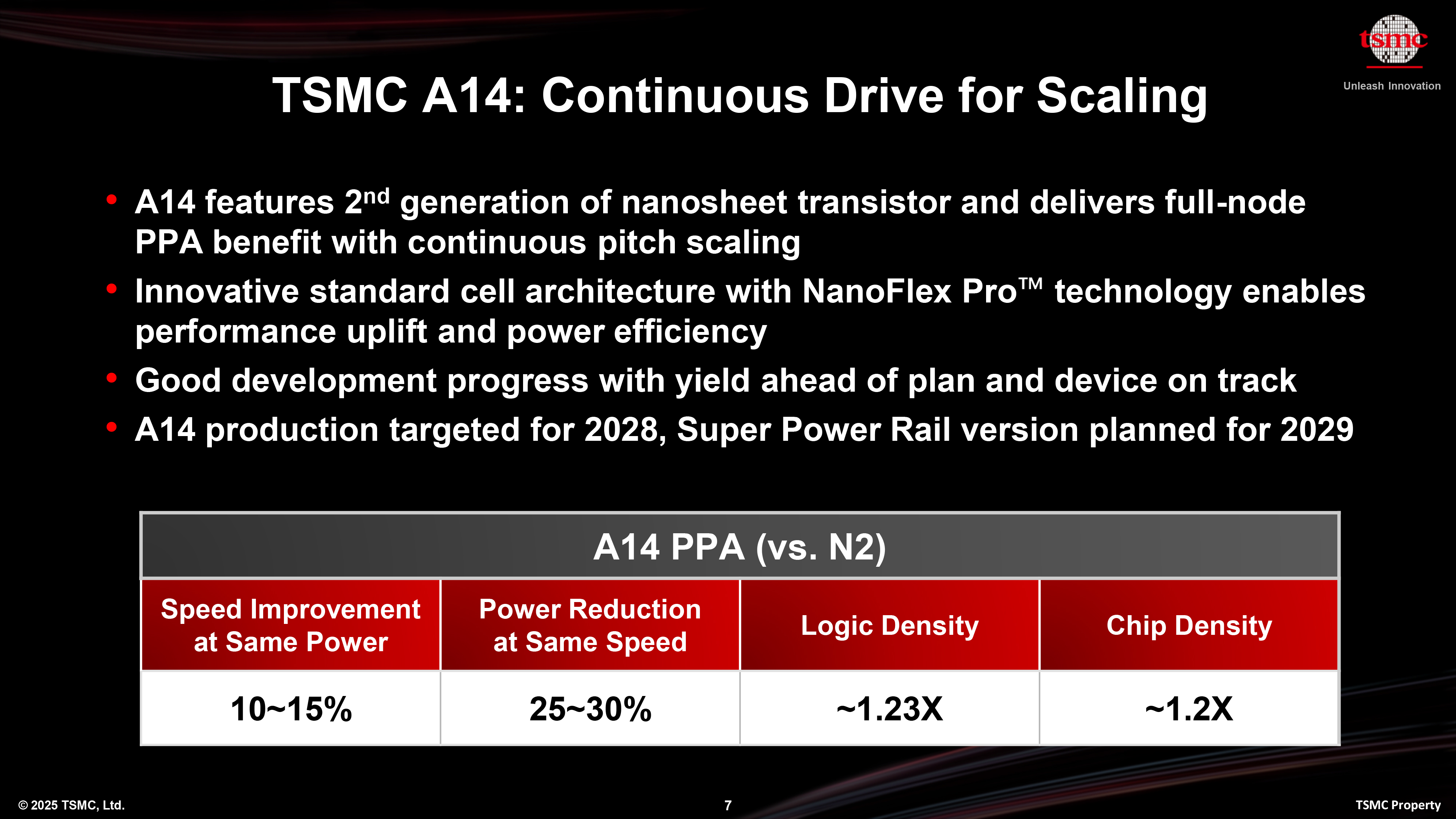
TSMC has revealed its A14 (1.4nm-class) manufacturing technology, which it promises will offer significant performance, power, and transistor density benefits over its N2 (2nm) process. At its North American Technology Symposium 2025 on Wednesday, the company disclosed that the new node will rely on its 2nd Generation gate-all-around (GAA) nanosheet transistors and will offer further flexibility with NanoFlex Pro technology. TSMC expects A14 to enter mass production in 2028 — but without backside power delivery. A version of A14 with backside power delivery is planned for 2029.
"A14 is our full-node next generation advanced silicon technology," said Kevin Zhang, senior vice president of business development and global sales and deputy COO at TSMC. "If you look at speed, enhancement [compared to N2] is up to 15%, power reduction is at 30%, logic density is 1.23x the overall chip density, or at least 1.2x [for mixed designs]. So, this is a very, very substantial technology."