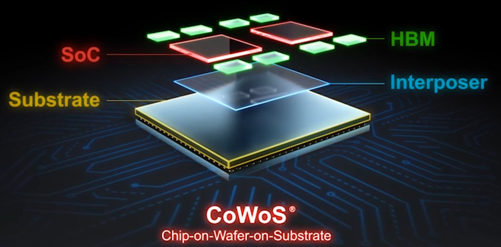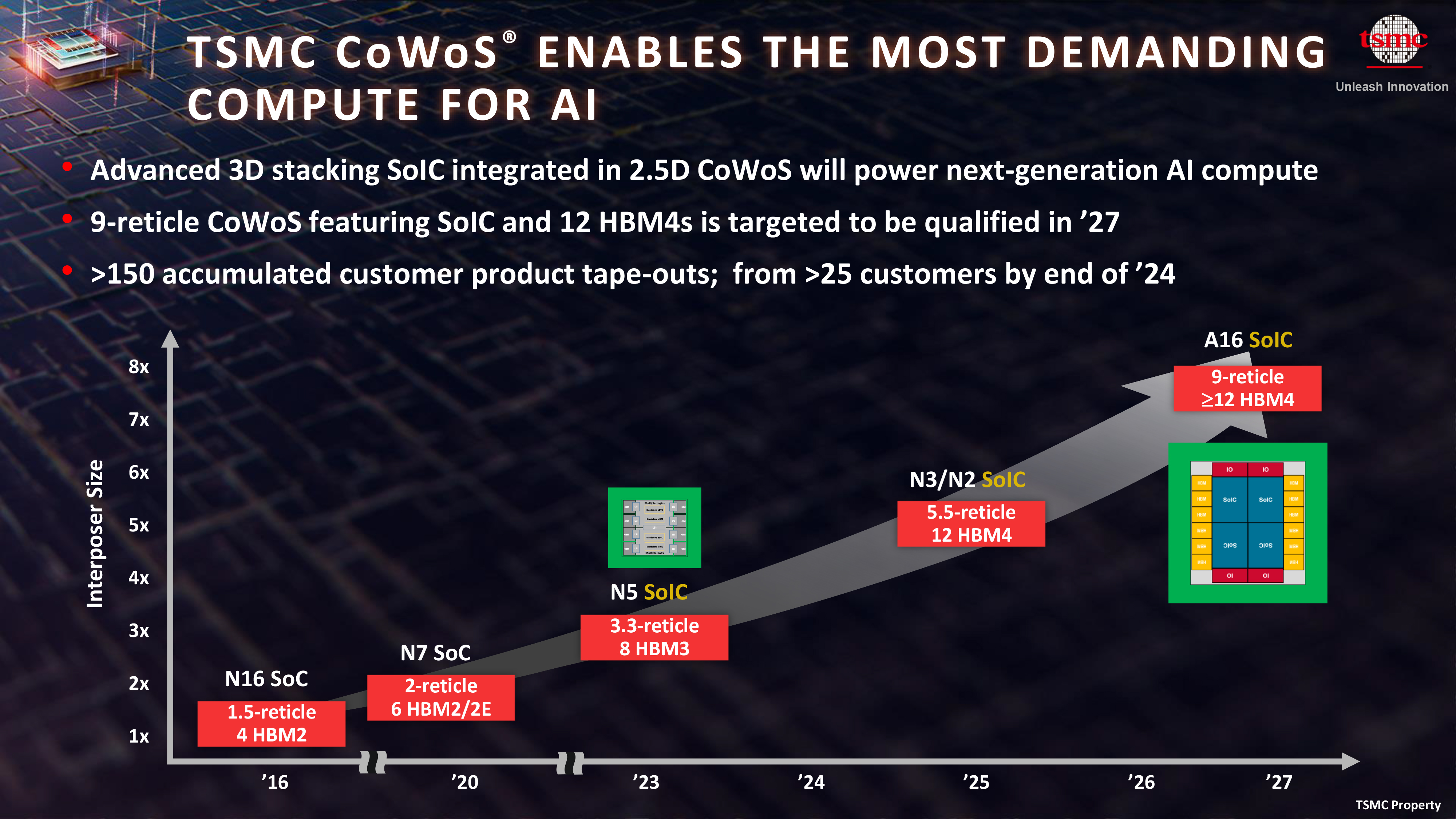
TSMC is on track to qualify its ultra-large version of chip-on-wafer-on-substrate (CoWoS) packaging technology that will offer an interposer size of up to nine reticle sizes and 12 HBM4 memory stacks in 2027, the company announced at its European Open Innovation Platform (OIP) forum this month. The new packaging method will address the most performance-hungry applications and let AI and HPC chip designers build processors the size of the palm of a hand.
TSMC introduces new process technologies every year, doing its best to meet its customers' needs for power, performance, and area (PPA) improvements. But some customers need even more performance, and for whom an EUV litho tool reticle limit of 858 mm^2 is not enough. These customers choose to use multi-chiplet solutions packaged using TSMCs CoWoS technology, and in recent years, the company offered multiple iterations of this method.

The original CoWoS enabled chip packages of around 1.5-reticle size in 2016, then evolved to 3.3-reticle size today, which enables placing eight HBM3 stacks into a package. Next up, TSMC promises 5.5-reticle size packages with up to 12 HBM4 memory stacks in 2025 – 2026. However, this pales behind the company's ultimate version of CoWoS, enabling system-in-packages (SiPs) of up to nine reticle sizes with 12 and potentially more HBM4 modules onboard.
That 9-reticle 'Super Carrier' CoWoS (offering up to 7,722 mm^2 for chiplets and memory) with 12 HBM4 stacks is planned to be qualified in 2027, so it is reasonable to expect it to be adopted in 2027 – 2028 for ultra-high-end AI processors.
TSMC fully expects companies adopting its advanced packaging methods to also vertically stack their logic using its system-on-integrated chips (SoIC) advanced packaging technologies to further boost transistor counts and performance. In fact, with 9-reticle CoWoS, TSMC expects its clients to place a 1.6nm-class die on top of a 2nm-class die, so we are talking about very high transistor density.
However, there is a major challenge with those ultra-large CoWoS packages. The 5.5-reticle CoWoS package will require an over 100x100 mm substrate (which is approaching the size constraints of the OAM 2.0 standard, which measures 102×165mm), whereas the 9-reticle CoWoS will go beyond a 120x120 mm substrate. Such major substrate dimensions will have an influence on how systems are designed and how data centers are equipped to support them. In particular, power and cooling. When it comes to power, we are talking about hundreds of kilowatts per rack, whereas when it comes to cooling, we are talking about liquid cooling and immersion methods to manage high-power processors effectively.


