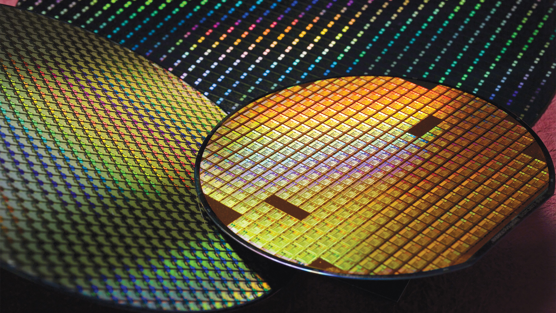
TSMC's N2 (2nm-class) manufacturing technology promises to provide numerous advantages over existing N3 (3nm-class) fabrication processes as it is set to adopt nanosheet gate-all-around transistors and NanoFlex. However, it will come at a much higher price than expected as the world's No.1 foundry will sell N2 wafers at a price that is roughly two times higher compared to a price of an N5 wafer, according to China Times. But there is a catch.
TSMC's quote for a 300-mm wafer process using its N2 technology will exceed $30,000, according to the report. Previously it was expected that world's largest contract maker of chips will charge around $25,000 per N2 wafer, up significantly from around $18,500 per N3 (3nm-class) wafer. If the information is accurate, an N2 wafer will cost two times more than an N4/N5 wafer, which is believed to cost around $15,000 today.
Since the information comes from an unofficial source, it should be taken with a grain of salt. It should also be noted that TSMC's prices depend on multiple factors, including volumes and customer. While some customers have to pay less per wafer, others have to pay more, so the $30,000 number is a very rough estimate.
TSMC's upcoming N2 fabrication process is set to offer several improvements compared to the current N3E manufacturing technology. It is projected to deliver performance gains of 10% to 15% (at the same power and complexity), while also cutting power consumption by 25% to 30% (at the same clocks and complexity). Furthermore, the shift to the N2 node will likely enhance transistor density by about 15% on average. In general, transition from N3E to N2 brings similar improvements as transition to N3B from N5.
However, TSMC's N2 will feature nanosheet GAA transistors that will enable chip designers to have a more precise control over performance and power of different units by altering channel width (increased width ups performance, reduced width reduces power consumption). Also, TSMC's N2 features NanoFlex capability that enables chip designers to combine standard cells from different libraries — high-performance, low-power, and high-density — within the same block to optimize performance, power, and die size.
But N2 will likely be costly for TSMC. The company is building two fabs to make chips on its 2nm-class process technology and is spending tens of billions of dollars on them buying ultra-expensive EUV lithography equipment (at around $200 million per tool) among other things. Also, N2 will use multiple innovative production techniques that will make it more expensive for TSMC than N3E. N2 will likely add more EUV litho steps in general, which will increase its costs. For example, TSMC might need to return EUV double patterning with N2, which will increase its costs, so it is reasonable for the foundry to pass these extra costs to its clients.
If the $30,000 per wafer quote is accurate, then it remains to be seen whether usage of N2 over N3 (to get 15% higher transistor density while also gaining performance and reducing power) will make a lot of economic sense for all of TSMC's customers. Apple is poised to use N2 in the second half of 2025 at it needs improved processors for iPhones, iPads, and Macs every year (though expect these products to get N2 chips only in 2026). Other large customers usually catch up with Apple in 1.5 – 2 years, so the quote might get a little lower by that time.
Then again development of 2nm-class system-on-chips is a very expensive endeavor, particularly because TSMC is moving on to nanosheet GAA transistors (which means all-new IP and design tools) and gives some extra controls over power, performance, and area, which potentially increases development costs. Therefore, chip designers who can afford developing a 2nm processor will likely be able to afford its production at $30,000 per wafer. Yet, expect them to pass those extra costs to the end user.


