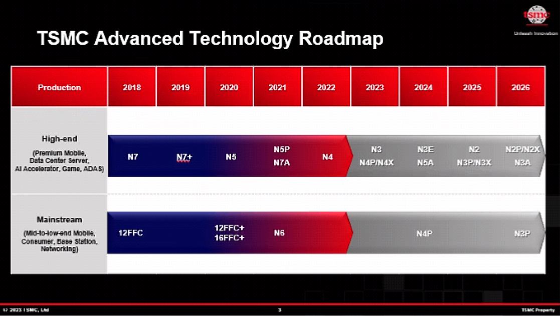
At the 2023 North American Technology Symposium TSMC revealed more information about its upcoming 2nm-class process technologies set to be production ready in 2025 – 2026. The world's largest foundry plans to expand its N2 family with N2P that will get a backside power rail and promises to boost performance, reduce power consumption, and increase transistor density. In addition, TSMC plans N2X, a node designed to deliver maximum performance and support for higher voltages.

N2 Provides Full Node Advantages
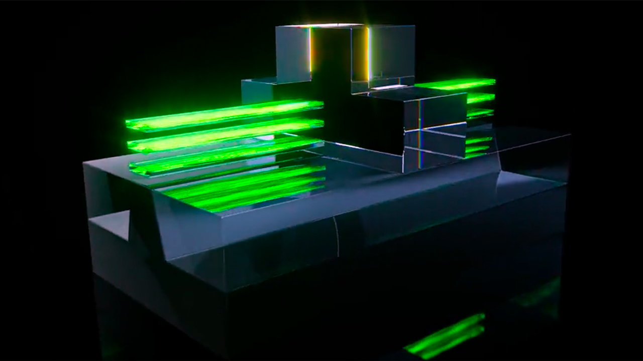
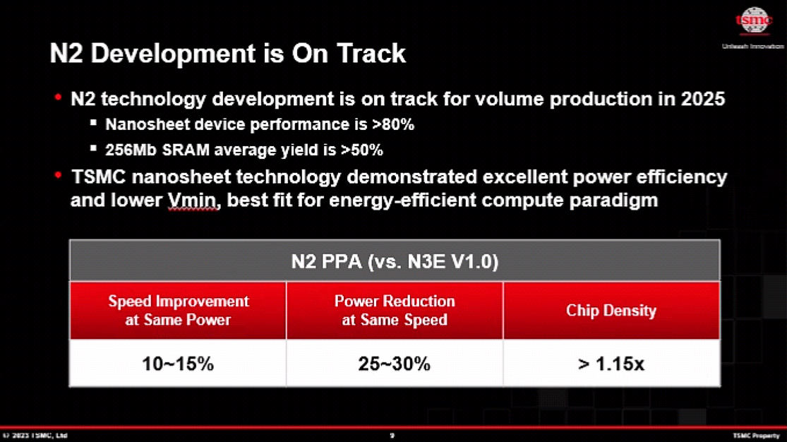
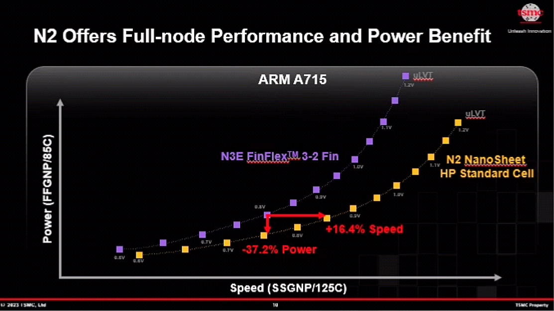
TSMC's original N2 process technology, set to enter high volume production sometime in 2025, introduces gate-all-around (GAA) Nanosheet transistors. When compared to N3E, the new node promises to boost performance by 10% to 15% with an identical power and transistor count, or decrease power consumption by 25% to 30% while maintaining the same frequency and complexity. When it comes to scaling, TSMC refrains of providing detailed numbers, but says that the new fabrication technology will enable an increase of chip density by 15%, which is an ambiguous term as it reflects a hypothetical IC containing 50% logic, 30% SRAM, and 20% analog circuits.

TSMC's N2 progress looks to be as planned. At its symposium, TSMC announced that its Nanosheet GAA transistor performance had reached over 80% of its target specifications and that the average yield of a 256Mb SRAM test IC exceeds 50%.
N2P: Backside Power Rail for Higher Performance Efficiency
While N2 provides tangible advantages over N3E, its successor N2P promises to be even more impressive. TSMC's second generation 2nm-class process is set to incorporate backside power delivery network (PDN) that is designed to increase transistor performance, lower power consumption, increase transistor density, and eliminate risks of interference between data and power wires in the chip.
Backside power delivery is one of the most important innovations in the recent years as back-end-of-line (BEOL) and contact resistances have been chipmakers' major challenges for a while. By relocating power rails to the back of the wafer, backside power delivery separates I/O and power wiring and mitigates elevated via resistance issues in the BEOL.

Though TSMC has not provided specific figures regarding N2P's performance, power, and area (PPA) benefits over N2, some analysts say that backside PDN could lead to a single-digit power consumption decline and double-digit transistor density increase. Keeping in mind that TSMC will likely make further optimizations to N2P, expect this technology to be significantly more advanced than N2 and N3 both in terms of performance efficiency and in transistor density.
TSMC expects N2P to be ready for high volume manufacturing (HVM) in 2026, so expect actual chips made on this node to ship in 2027. Assuming that Intel fulfils its promise and ships the first chips made on its 20A production technologies (which employs both RibbonFET GAA transistors and PowerVia backside PDN) in 2024, it will be two or three years ahead of TSMC with backside power rail.
N2X: High Voltages for Extreme Performance
TSMC is developing N2X, a fabrication process tailored for high-performance computing (HPC) applications such as high-end datacenter CPUs. In general, these chips are power hungry and need the ability to increase their clocks at peak demands. This means that they have to support high voltages and currents. Since the node is set to be available in 2026 at the earliest, TSMC does not outline its performance enhancements over N2, N2P, and N3X just now. Meanwhile, as with all recent production technologies, maximum performance and efficiency can only be achieved through extensive design technology co-optimization (DTCO) between foundry and IP developers.


