
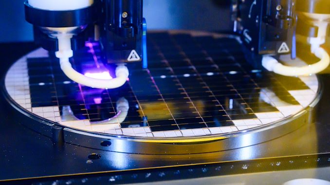
TSMC is no stranger to building big chips. Besides the ~800mm2 reticle limit of their normal logic processes, the company already produces even larger chips by fitting multiple dies on to a single silicon interposer, using their chip-on-wafer-on-substrate (CoWoS) technology. But even with current-gen CoWoS allowing for interposers up to 3.3x TSMC's reticle limit, TSMC plans to build bigger still in response to projected demand from the HPC and AI industries. To that end, as part of the company's North American Technology Symposium last week, TSMC announced that they are developing the means of building super-sized interposers that can reach over 8x the reticle limit.
TSMC's current-generation CoWoS technology allows for building interposers up to 2831 mm2 and the company is already seeing customers come in with designs that run up to those limits. Both AMD's Instinct MI300X accelerator and NVIDIA's forthcoming B200 accelerator are prime examples of this, as they pack huge logic chiplets (3D stacked in case of AMD's product) and eight HBM3/HBM3E memory stacks in total. The total space afforded by the interposer gives these processors formidable performance, but chip developers want to go more powerful still. And to get there as quickly as possible, they'll need to go bigger as well in order to incorporate more logic chiplets and more memory stacks.