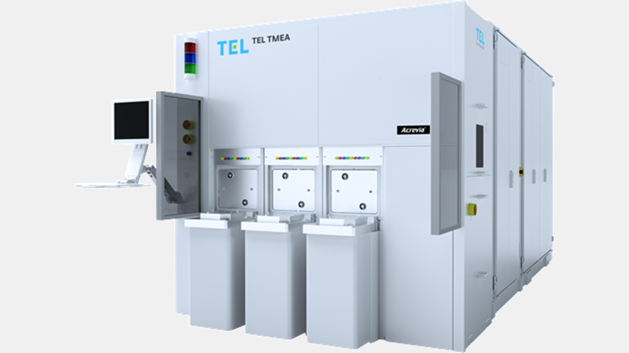
Tokyo Electron has introduced its Acrevia, a new gas cluster beam (GCB) system tailored for refining patterns created by EUV lithography. The tool, which uses low-damage surface processing, can be used for several things, including reducing the usage of EUV multi-patterning for upcoming nodes, enhancing line edge roughness to reduce performance variability, reducing stochastic litho defects, and ultimately cutting chipmaking costs and improving yields.
Modern EUV lithography tools with 0.33 numerical aperture optics (Low-NA EUV) can achieve critical dimensions of 13 nm to 16 nm for high-volume production with a single exposure. Printing a 26-nm minimum metal pitch is enough, acceptable for 3nm-class process technologies. To print finer circuits with smaller metal pitches for 2nm-class production nodes and beyond, chipmakers have to either use an EUV lithography machine with a 0.55 numerical aperture optics (High-NA EUV), Low-NA EUV double patterning, Applied Materials’s Centura Sculpta pattern shaping tool, or, now Tokyo Electron’s Acrevia.