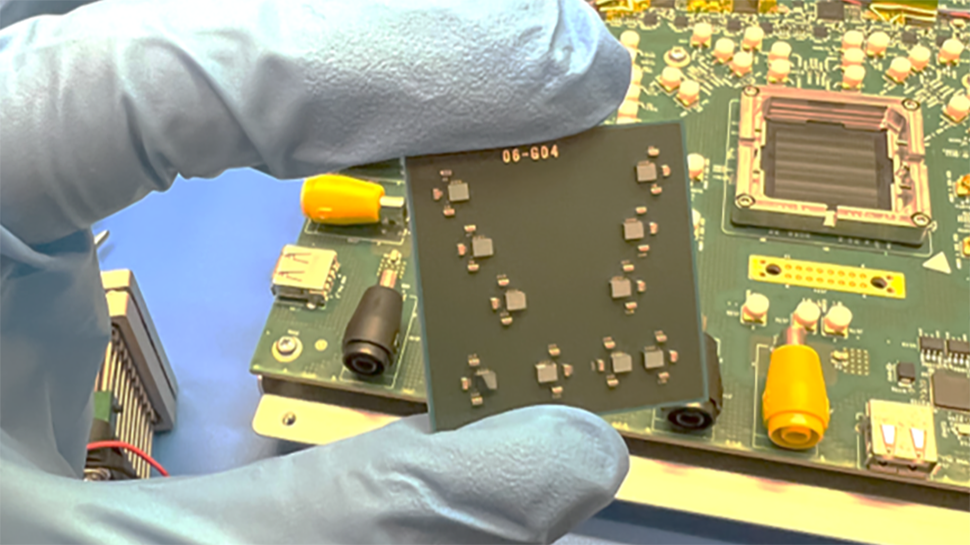
Many system designers are exploring chiplet-based SiPs that move beyond the limitations and costs of huge single-die implementations, but which depend heavily on silicon interposers as substrates for mounting and interconnecting the dies.
Silicon interposers deliver a higher data rate than organic substrates, but are not without drawbacks. They are costly, proprietary and limit the number of chiplets that can be placed on one substrate due to size restrictions, while increasing TCO.
Many CPUs are multi-die assemblies which make use of organic substrates (implemented using chiplet interconnect standards like UCIe and the Open Compute Project’s Bunch of Wires (BoW)), but they can’t compete performance-wise with silicon interposers.
Build a better ‘Blackwell’
Now, Eliyan has come up with what it believes is a viable solution that offers the performance advantages of silicon interposers but without their limitations. The solution to this dilemma, the firm says, is to look at the dies themselves - "at the tiny electronic circuits that drive the interconnect lines”. Most of today’s chiplet interconnect standards use a physical-layer (PHY) IP block, but Eliyan’s NuLink PHY reportedly reaches the same maximum performance levels on organic substrates that alternative PHYs can only achieve on silicon interposers.
The company says NuLink PHY, “enables systems with higher performance (more memory) and lower TCO (no interposer),” with results that deliver up to 4x the bandwidth, 4x the power efficiency, up to 4x the SiP size and up to 10x the AI performance.
Eliyan’s Co-founder and chief executive officer Ramin Farjadrad recently talked to The Next Platform about how NuLink PHY can be used to “build better, cheaper, and more powerful compute engines than can be done with current packaging techniques based on silicon interposers.”
The article, titled “How To Build A Better ‘Blackwell’ GPU Than Nvidia Did”, explains how its technology could be used to significantly improve on Nvidia’s superchip design.
It’s a fascinating read, and hints at what could be possible in the future. As The Next Platform’s Timothy Prickett Morgan sums up, “Any memory, any co-packaged optics, any PCI-Express or other controller, can be linked using NuLink to any XPU. At this point, the socket really has become the motherboard.”
There’s certainly a lot of interest in Eliyan’s NuLink PHY. The company recently closed a $60 Million Series B funding round, co-led by Samsung Catalyst Fund and Tiger Global Management. “This investment reflects the confidence in our approach to integrating multi-chip architectures that address the critical challenges of high costs, low yield, power consumption, manufacturing complexity, and size limitations,” Farjadrad said, following the funding announcement.


