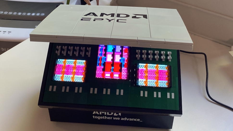
For decades, the number of transistors that could be squeezed onto a single piece of silicon had increased on the principle of Moore’s Law, an observation that the speed and capability of computers can be expected to double every two years. However, in recent years Moore's Law has slowed down significantly, forcing the semiconductor industry to look for different ways to boost the performance and efficiency of CPUs.
In 2018, a new type of chip design that many hailed as an industry breakthrough in performance and scalability made its debut. AMD debuted this new “chiplet” technology in the AMD “Zen 2”-based 2nd Gen EPYC server processor (formerly codenamed “Rome”), which will go down in history as the first processor to feature a revolutionary chiplet-based x86 CPU design.
Building on a concept that dates back to at least 1965, this chiplet-based approach meant that instead of being built on a single die and engineered from scratch, chips could be composed of multiple smaller pieces – or chiplets – that are then “stitched” together as one.
The introduction of chiplets - which some have likened to hi-tech Lego - solved many problems for the semiconductor industry. Shifting to a chiplet-based design can lower manufacturing costs, enabling chipmakers to create entire lineups of server products without redesigning for each end market.
What are the benefits of chiplets?
Chiplets are small, modular chips that can be combined to create a larger, more powerful processor package. In simple terms, this new approach allows companies to use smaller die instead of one large, monolithic piece of silicon. These smaller die yield better in manufacturing than larger die, meaning a larger proportion of the die produced are considered viable. This reduces manufacturing losses, and therefore production costs. It allows companies to offer vastly increased core densities, enabling much higher compute and memory performance than a monolithic chip.
Chiplets also allow the processor to be built up in modular fashion. For instance on the EPYC 7002 and 7003 series processors, there is a central I/O die surrounded by up to 8 compute chiplets. This allows the core count of the CPU to scale from 8 to 64 cores, whilst ensuring that costs are optimised where possible to ensure value for the customer. If the core count doesn’t require all 8 chiplets, then either 2, 4 or 6 chiplets will be used, which means the customer won’t be paying for unused silicon.
This also allows the design and manufacturing processes to be simplified – in order to build an entire stack of products from 8 to 64 cores, AMD need only produce 2 devices – the I/O die and the compute chiplet – and then populate the package with as many as are needed. To build the same stack on a monolithic technology would likely require 4 or 5 different devices to be produced to suit the variety of core counts.
There is also no reason why the chiplets have to be used for x86 compute. It would be possible, for instance, to replace an x86 compute chiplet with one designed specifically as an AI accelerator, or a network offload engine, or any other dedicated device. This opens up enormous potential for addressing emerging workloads, without compromising the core compute requirement that customers demand.
Another advanced packaging mechanism that can be used to push the boundaries of performance is die stacking. This allows die to be stacked vertically on top of one another, rather than being distributed on the same package with longer interconnects between them. This reduces latency and improves performance. AMD has pioneered die stacking technologies with the introduction of 3D V-Cache, which uses stacked die to triple the amount of L3 cache on a CPU.
What’s next for chiplets?
What AMD accomplished with the introduction of its second generation EPYC processors five years ago is now on its way to becoming the industry norm. Many of the biggest names in the semiconductor industry are moving towards chiplet-based designs as they realise that, as monolithic designs cease to scale, a new approach is needed.
This means that we’re starting to see chiplets enter the supercomputer race. The world’s current fastest supercomputer, Frontier, is built on a chiplet-based CPU, which allowed it to be the first supercomputer to break the Exaflop barrier. The upcoming El Capitan machine will utilise chiplet-based CPUs and GPUs, and is expected to exceed 2 Exaflops. This new approach to chip design enables a new class of systems that continue to scale in performance at the cutting edge, and indeed 4 of the current top 10 supercomputers globally are built on an AMD EPYC chiplet-based solution.
Chiplets are even making it into the technologies that we use every day. Chipmakers have begun using a chiplet-based approach in graphics cards, as the scalable microarchitecture that can be applied easily to different segments.
So what’s next? Several of the largest chipmakers, including AMD are backing a new standard for connecting chiplets made by different companies. The “Universal Chiplet Interconnect Express” or “UCIe” could reshape new semiconductor designs, intended to enable chipmakers to mix and match silicon from different vendors inside a single package.
No matter what is around the corner, it’s clear that the introduction of chiplets continues to inspire the semiconductor industry to innovate.


