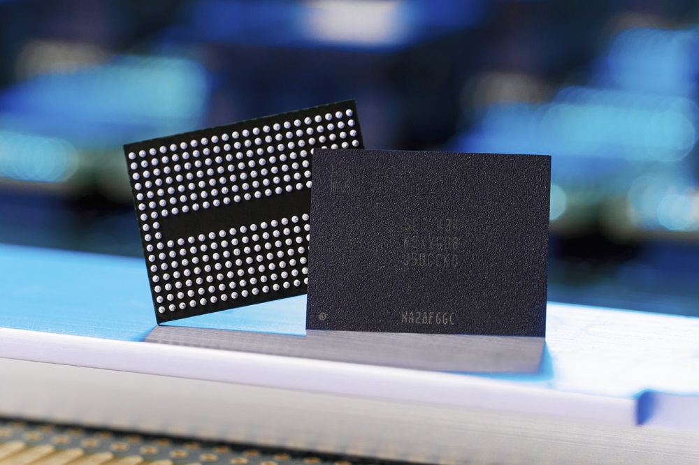
With the arrival of 3D NAND about a decade ago, the storage capacity of solid-state drives has been increasing rapidly, and the per-GB price has been decreasing steadily. It is why the vast majority of client PCs use SSDs these days. IEEE believes this trend will continue in the coming years, increasing SSD storage capacity to at least quadruple by 2029.
The reason 3D NAND has been increasing capacity is multifaceted. On the one hand, the number of active NAND layers has increased over the years, and on the other hand, the number of bits stored per NAND memory cell has increased from two to three (triple-level cell, TLC) and four (quad-level cell, QLC). Both innovations have happened over time and were meticulously calculated to achieve economic targets regarding per-TB costs.
We live in 2024. 2Tb QLC NAND memory devices are readily available to enable some of the world's best mainstream 2TB SSDs, which gives them 2TB of raw storage space. IEEE's roadmap pins 4Tb 3D NAND devices to 2027, doubling the capacity for mainstream SSDs. Then, the capacity is expected to quadruple in 2029 as the industry migrates to 8Tb NAND memory devices. That given, expect the capacity of mainstream SSDs to quadruple by 2028, though we are speculating.

Regarding the number of active layers, we are in the midst of 200 and 300 layers, depending on the manufacturer, but IEEE predicts 500+ in 2027. Then companies like Samsung and SK hynix predicted 1000+ layers, which the respected institute decided to avoid predicting.
Unlike predictions for the evolution of hard drives, the new IEEE International Roadmap for Devices and Systems Mass Data Storage roadmap is vague regarding what is to be achieved regarding storage density. And the number of active NAND layers and other NAND memory architectures. IEEE does not even call QLC as QLC; it calls it TLC+, perhaps implying possibilities beyond even QLC (4-level charge), possibly to 5-level charged PLC (penta level cell).
"The path to continuing increasing the die density and reducing the cost per bit will involve minimizing the growth in layer count, increasing the density of memory cells per layer (increasing the areal density per layer), decreasing the size of the holes where the memory cells are manufactured, increasing the number of bits stored per transistor [triple-level cell (TLC) to QLC to PLC], and maintaining a uniform high aspect ratio etch for each memory hole. These are design and manufacturing issues and must be solved to maintain the high production yields necessary for profitable manufacturing."


