There's a freshly leaked image of a Radeon chiplet GPU design—reportedly from a now-cancelled Navi 4C die—and it's rocking anywhere between 13 and 20 different chiplets on one GPU. I love a bit of ambition, but I think we're starting to see why AMD really might be calling time on competing at the high end in its next graphics card generation.
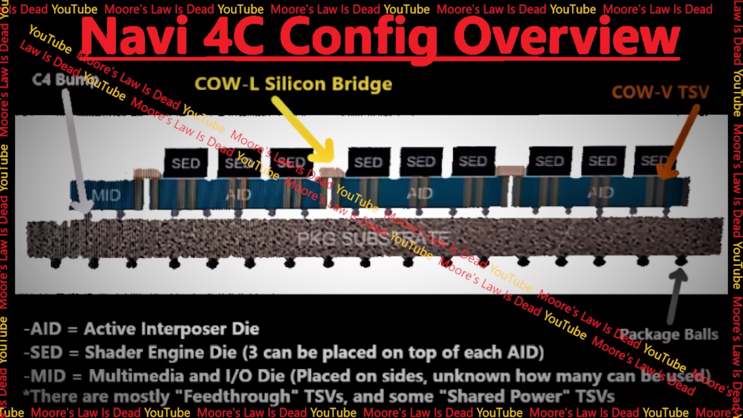
The GPU design schematic has come from the Moore's Law is Dead channel (via Videocardz) and shows a hugely more complex chiplet design than we've seen in the current Navi 31 silicon that powers the Radeon RX 7900 XTX. That was the first chiplet GPU in the gaming space, and honestly I thought it was a minor miracle AMD had managed to get the card working as well as it did as a gen1 implementation of the tech.
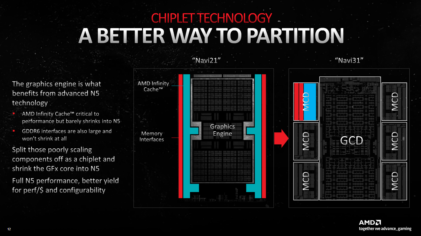
It must be said, though, that it wasn't necessarily a true chiplet design in the same vein as AMD's recent Ryzen processors. Those processors use multiple compute chiplets—multiple dies with multiple CPU cores on each—along with an accompanying I/O die to take care of the interconnects. The approach with the latest Radeon, on the other hand, is still chiplet-based, but only contains a single compute die with separate memory cache dies as the discrete chiplets.
This leaked Navi 4C design, however, is something else entirely. It's an order of magnitude more complex, with multiple compute chiplets as well as separate I/O and memory chiplets, all arrayed on a single substrate.
The image displayed on the Broken Silicon show only has one horizontal shot of the design, and even then it's showing 13 distinct chiplets, with MLID stating there will be memory controller chips not shown in the image, which could push the figure up to 20 or more.
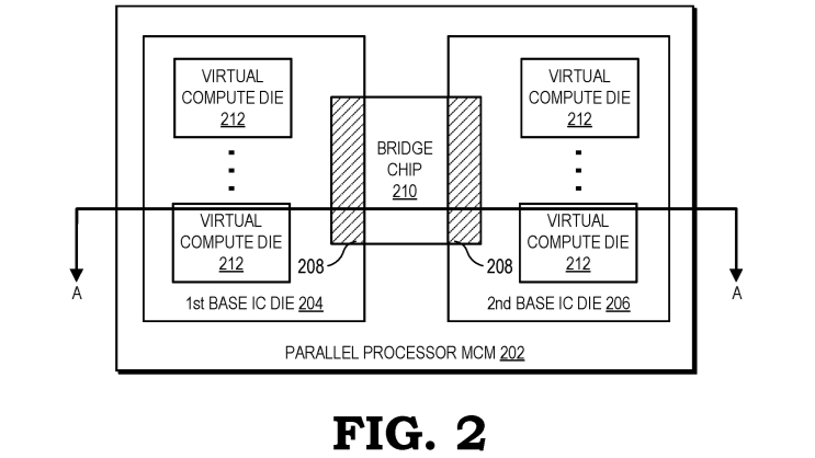
By way of confirming the veracity of the image, they also highlight a patent from 2021—Die stacking for modular parallel processors (PDF warning)—which seemingly talks about this design, and has images which look a lot like that shown in the video.
And if they are talking about the same design, we could even be looking at way more chiplets, as the patent shows a bridge chip connecting a pair of base IC dies. Basically, there could be another 13 chiplets on the other side of those shown in the cross-section. The numbers are wild and, honestly, so is the ambition AMD shows in trying to pull this off.


But MLID explains that it is now able to show this particular image off because the GPU design has now been cancelled, which is as much a pity as it is unsurprising.
We've previously spoken about how AMD's next generation of GPUs is unlikely to arrive with high-end parts, and it looks like it's now only going to come with the mainstream and thoroughly monolithic Navi 43 and Navi 44 chips.
That's not necessarily AMD going backwards, giving up on chiplets having tried once in RDNA 3 and failing in RDNA 4. The reports are that it's refocusing its engineers on RDNA 5—probably for the back-end of 2025 at the earliest—and I would be very surprised if that wasn't in order to get a proper multi compute die chiplet GPU in place at the very high end of its next next-generation graphics card range.
Well, so long as it can get it to work, that is. Getting multiple compute chiplets to work together on gaming graphics is a lot harder than getting them to do classic CPU number-crunching. Just ask anyone who ran an SLI or CrossFire rig back in the day.
Admittedly, it's still not a great look for AMD to only bring out half a generation next time around, but better it can figure out the problems with its design now and work on a better solution for RDNA 5. Though it would've been handy if it had a contingency plan, like maybe a new node for a refreshed Navi 31 perhaps.


