
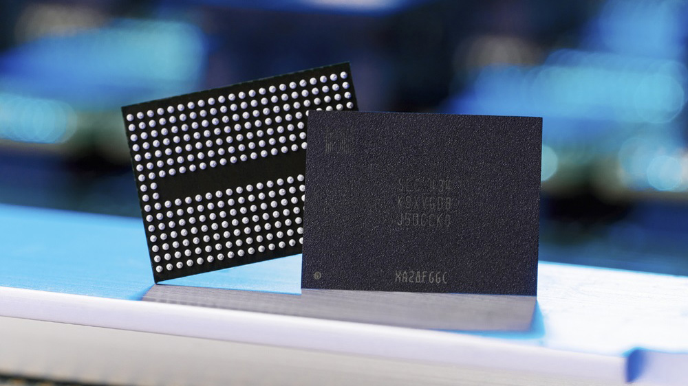
Samsung has introduced its upcoming 10th-generation V-NAND flash memory with over 400 active layers and a 5.6 GT/s interface speed at the International Solid-State Circuit Conference 2025. The new type of memory not only boasts a record number of active layers and groundbreaking performance (which will enable some of the best SSDs), but it also uses Samsung's cell-on-peripheral (CoP) architecture with hybrid bonding, a first for Samsung.
The 10th Gen V-NAND device that Samsung presented at ISSCC is a 3D TLC NAND device with over 400 active layers, a 1 Tb capacity per die, and a 5.6 GT/s interface speed. As the new memory IC continues to use a triple-level cell design, it offers a 28 Gb/mm^2 density, which is slightly lower compared to Samsung's 1Tb 3D QLC V-NAND, which reaches 28.5 Gb/mm^2. However, density may not be Samsung's main goal with this particular product as the key innovations that it introduces are the record number of active layers (over 400) and hybrid bonded periphery circuitry.