
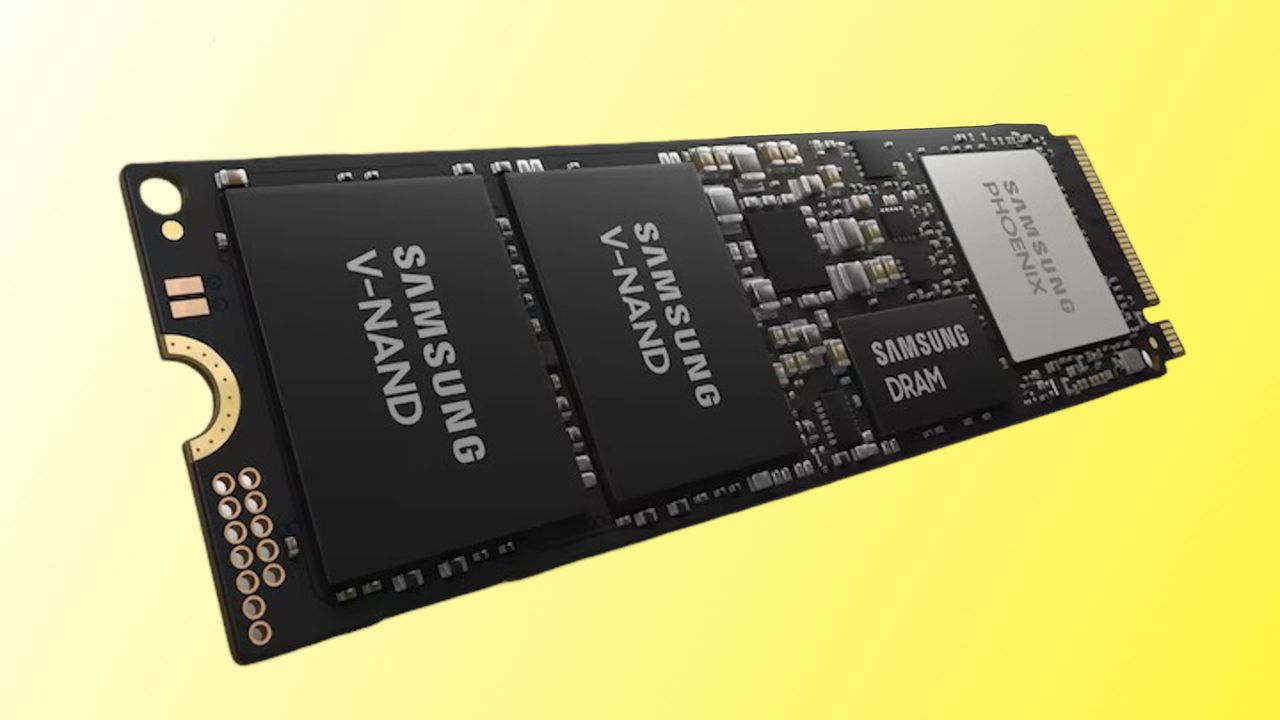
Samsung has developed a new prototype NAND memory chip composed of an incredible 900 layers, according to a new report. The chip is actually achieved by stacking two 450-layer cell wafers.
ET News (via Sammobile) says, "Samsung Electronics recently implemented a 900-layer Class V-NAND integrated system utilizing Cell Multi-Bonding (CMB) technology, which bonds two 450-layer cell wafers into one."