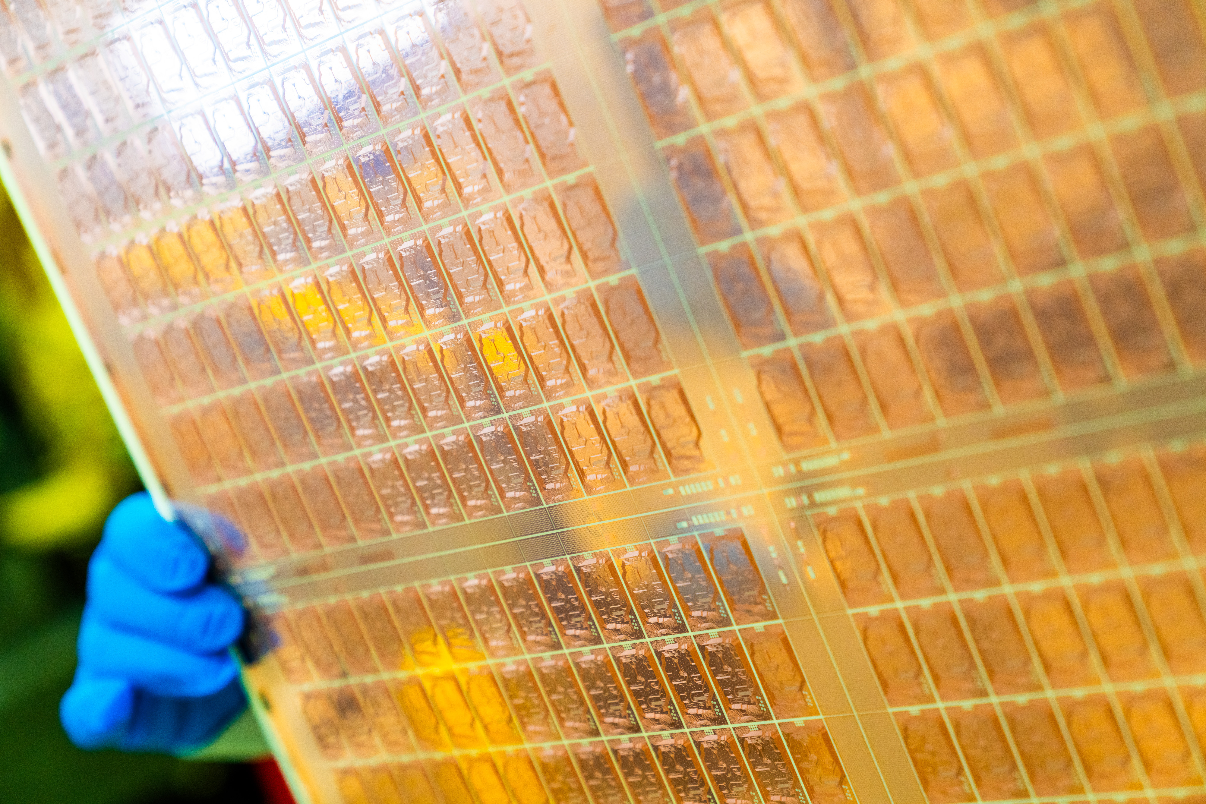
Samsung Electro-Mechanics is fast-tracking its venture into the semiconductor glass substrate market, advancing its equipment procurement and installation to September and starting to operate its pilot line in the fourth quarter, a quarter ahead of the initial plan, reports ETNews. The company expects to start production of glass substrates for high-end system-in-packages (SiPs) in 2026. To land orders for 2026, the company needs to demonstrate decent capabilities in 2025.
To build highly-complex multi-chiplet SiPs, Samsung needs to gain expertise in glass substrates. Therefore, the company's decision to move up the timeline for its pilot line at Sejong, South Korea, fab could be a strategic one and could reflect the growing importance of advanced chip packaging technologies for Samsung as well as the company's aggressive attempt to capture market share from Intel, which is on track to start offering advanced packaging on glass substrates in the coming years.
According to the report, Samsung Electro-Mechanics plans to have all necessary equipment installed at the pilot line by September and start operating it in the fourth quarter.
The selection of suppliers has been finalized, and companies like Philoptics, Chemtronics, Joongwoo M-Tech, and Germany’s LPKF have been tasked with providing components for the setup. The report said that this setup is designed to streamline production and adhere to Samsung's stringent safety and automation standards.

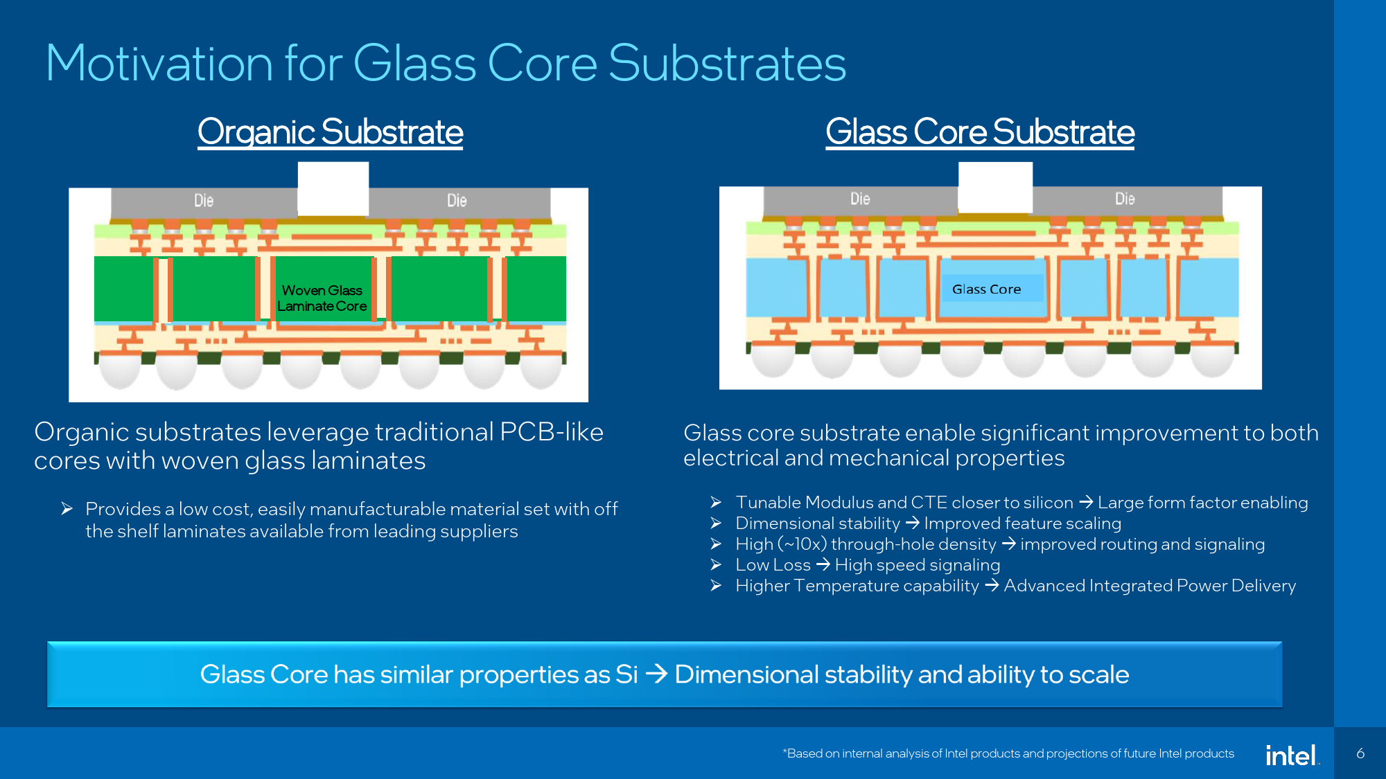
Glass substrates offer significant advantages over traditional organic substrates, including superior flatness that improves lithography focus and excellent dimensional stability for interconnects in next-generation SiPs with multiple chiplets. Additionally, they have better thermal and mechanical stability, making them suitable for high-temperature, durable applications in data centers.
Intel, which has been developing glass substrates for nearly a decade, plans to use them in commercial products by 2030. The company believes these characteristics will greatly enhance interconnect density, crucial for efficient power delivery and signal routing in advanced SiPs. Meanwhile, Absolics, a U.S.-based subsidiary of SKC, aims to make glass substrates for its clients as early as the second half of 2024.
As Samsung Foundry tries to land more orders from developers of data center-grade processors, the company needs to offer advanced packaging services as well. To that end, the glass substrates-related efforts of Samsung Electro-Mechanics (actually, the whole Samsung) could be crucially important for Samsung Foundry sooner rather than later.


