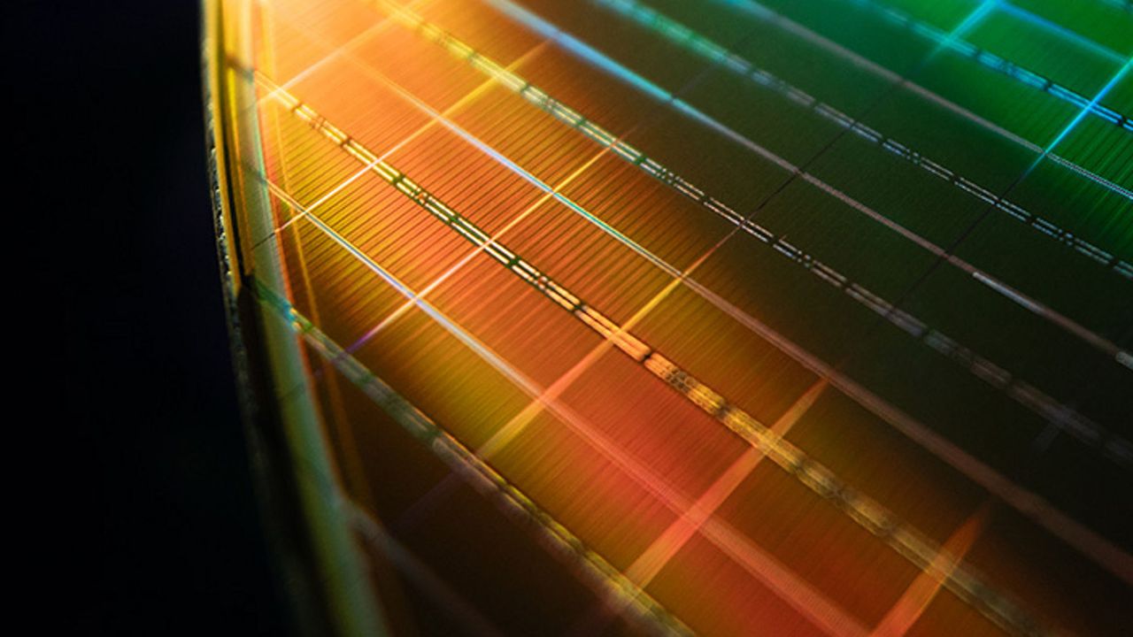
The Institute of Microstructure Physics of the Russian Academy of Sciences (via Dmitrii Kuznetsov) has laid out a long-term roadmap for domestic extreme ultraviolet (EUV) lithography tools operating at a wavelength of 11.2 nm, extending the information the organization shared last December. The new project spans from 2026, utilizing 40nm manufacturing technology, and extends to 2037, incorporating sub-10nm fabrication processes. The latest roadmap looks more realistic than some previous ones, yet it still has to prove itself to be executable. Furthermore, if executable, it may not be used for commercial purposes.
The very first thing that strikes the eye is that the proposed EUV* systems avoid replicating the architecture of ASML's tools. Instead, the plan is to use an entirely different set of technologies: hybrid solid-state lasers, xenon plasma-based light sources, and mirrors made from ruthenium and beryllium (Ru/Be) that reflect light at a 11.2nm wavelength. The choice of xenon instead of tin droplets in ASML's EUV tools eliminates debris that harms photomasks, which dramatically reduces maintenance. Meanwhile, when compared to ASML's DUV tools, the lower complexity is meant to avoid high-pressure immersion fluids and multi-patterning steps for advanced nodes.