Samsung is set to introduce 3D packaging services for high-bandwidth memory (HBM) this year, according to a report from the Korea Economic Daily that cites the company's announcement at the Samsung Foundry Forum 2024 in San Jose, as well as 'industry sources.' The 3D packaging for HBM essentially paves the way for HBM4 integration in late 2025 – 2026, but we are not sure what kind of memory Samsung is set to package this year.
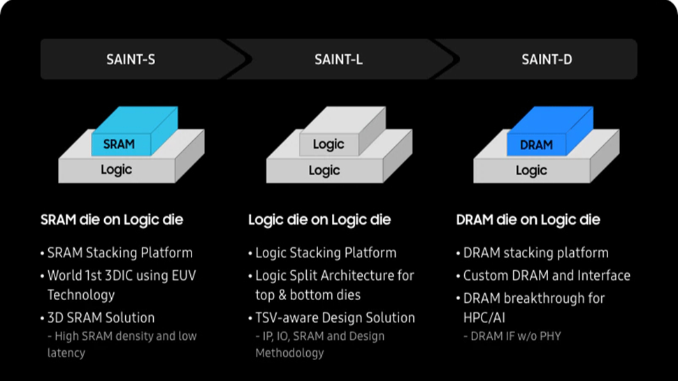
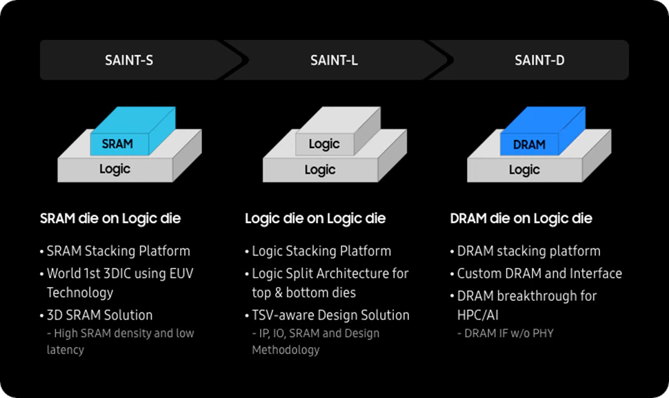
For 3D packaging, Samsung has a platform called SAINT (Samsung Advanced Interconnect Technology) that includes three distinct 3D stacking technologies: SAINT-S for SRAM, SAINT-L for logic, and SAINT-D for DRAM stacking on top of logic chips like CPUs or GPUs. The company has been working on SAINT-D for several years (and formally announced it in 2022) and it looks like the technology will be ready for prime time this year, which will be a notable milestone for the world's largest memory maker and a leading foundry.

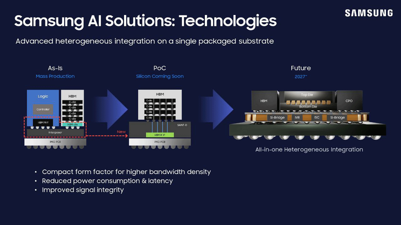
Samsung's new 3D packaging method involves stacking HBM chips vertically on top of processors, which differs from the existing 2.5D technology that connects HBM chips and GPUs horizontally via a silicon interposer. This vertical stacking approach eliminates the need for the silicon interposer but requires a new base die for HBM memory that is made using a sophisticated process technology.
The 3D packaging technology offers significant benefits for HBM, including faster data transfers, cleaner signals, reduced power consumption, and lower latencies, but at relatively high packaging costs. Samsung plans to offer this advanced 3D HBM packaging as a turnkey service, where its memory business division produces HBM chips, and the foundry unit assembles actual processors for fabless companies.
What remains unclear is what exactly Samsung plans to offer with SAINT-D this year. Putting HBM on a logic die requires an appropriate chip design and we are not aware of any processors from well-known companies that are designed to hold HBM on top and are set to launch in 2024 – 1H 2025.

Looking ahead, Samsung aims to introduce all-in-one heterogeneous integration technology by 2027. This future technology will enable the integration of two layers of logic chips, HBM memory (on interposer), and even co-package optics (CPOs).


