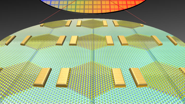
Korean researchers have developed a method to grow sub-nanometer semiconductor logic circuits. The team from the Institute for Basic Science (IBS) claims that they grew 1D metallic materials with a width of less than 1nm and developed them into 2D circuits. In effect, the 1D metals acted as a gate electrode of an ultra-miniaturized 2D transistor.
The headlining technology could be very important, as it exceeds predictions outlined on the International Roadmap for Devices and Systems (IRDS) by the IEEE. While the IEEE predicted semiconductor node technology to reach around 0.5 nm by 2037 with transistor lengths of 12nm, the IBS researchers demonstrated a 1D MTB (mirror twin boundary) gate can be as small as 3.9nm.