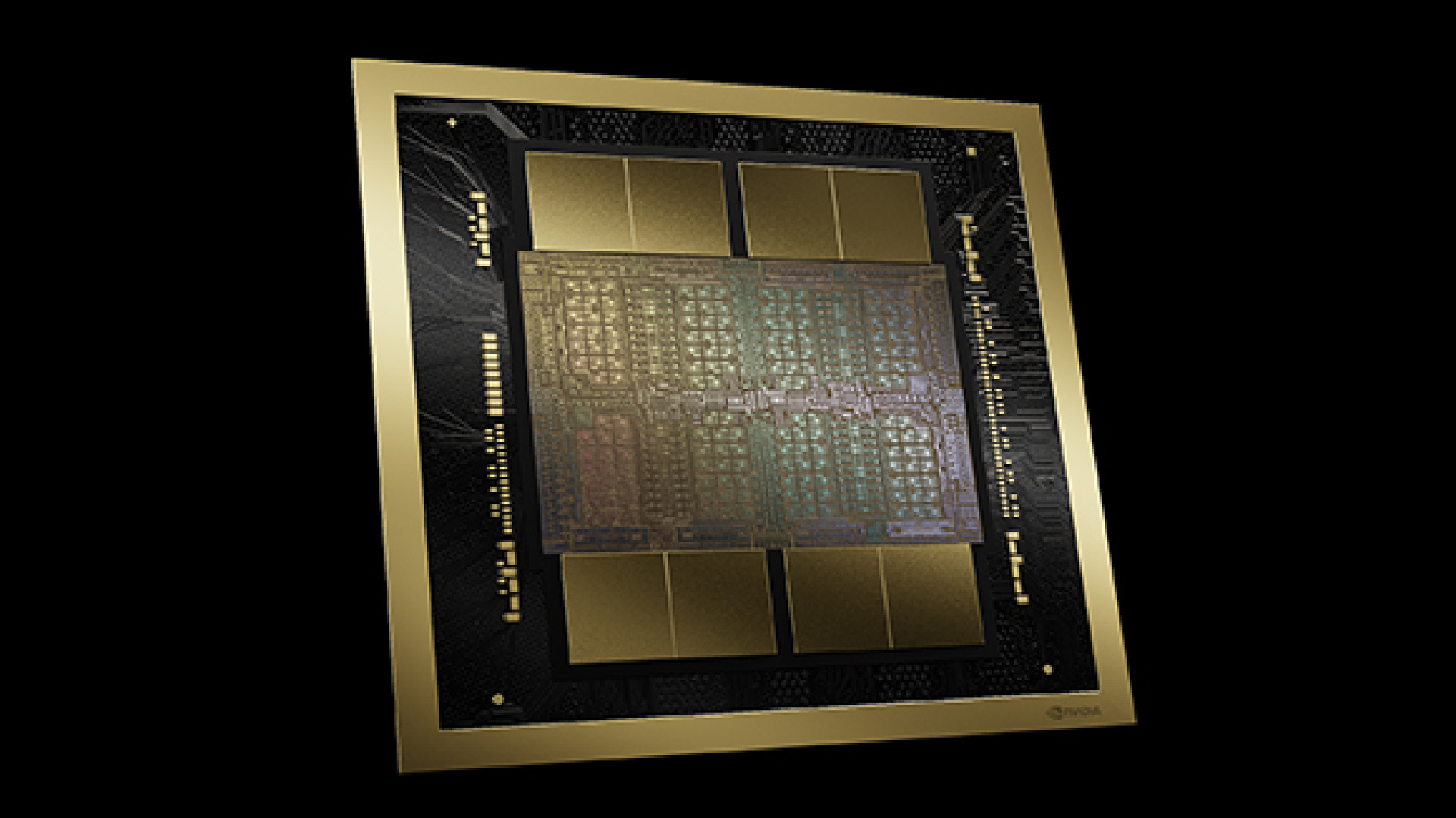
So, Nvidia's new AI monster is out, all 208 billion transistors of it. And immediately it's raising some tricky questions about what the hell Nvidia's upcoming Blackwell RTX 50-series graphics chips are going to look like.
From a gaming graphics perspective, many of the technicalities of Nvidia's new AI GPU aren't hugely relevant. However, there were two key pieces of information from the Nvidia Blackwell AI launch. First, it uses the existing TSMC N4 node—albeit a custom 4NP version—not one of the new TSMC N3 nodes. Second, it uses multi-die engineering, with two chips making up a single Blackwell AI GPU.
That's intriguing on about eight different levels all at the same time. So, let's try to break down some of the issues at play. It's all about transistor densities, production nodes, yields, and costs.
The current AD102 GPU in the RTX 4090 is created using a single die made on a custom TSMC 4N node. TSMC N5 and N4 are essentially variants of the same node with roughly similar specifications—like transistor density, reticle limits and so on—and this custom process is based on those.
Now, AD102 is a 76 billion transistor GPU. Its predecessor, the AD102 chip in the RTX 3090 contained 45 billion transistors and the TU102 in the RTX 2080 Ti was a mere 19 billion transistors. So, you can see how the transistor count has been scaling with each generation. Meanwhile, each die in the new Blackwell AI GPU is 104 billion transistors and said to be right at the limit of what is possible on the TSMC N4 node.
Current rumours around the upcoming RTX 5090 graphics card claim it will rock 175 SMs, or streaming multiprocessors. The RTX 4090 or AD102, for context, has 128 SMs. The full AD102 chip actually has 144 SMs, with some disabled to improve production yields and reduce costs. By only enabling 128 SMs, it means some AD102 dies with broken SMs can still be usable in RTX 4090 boards.
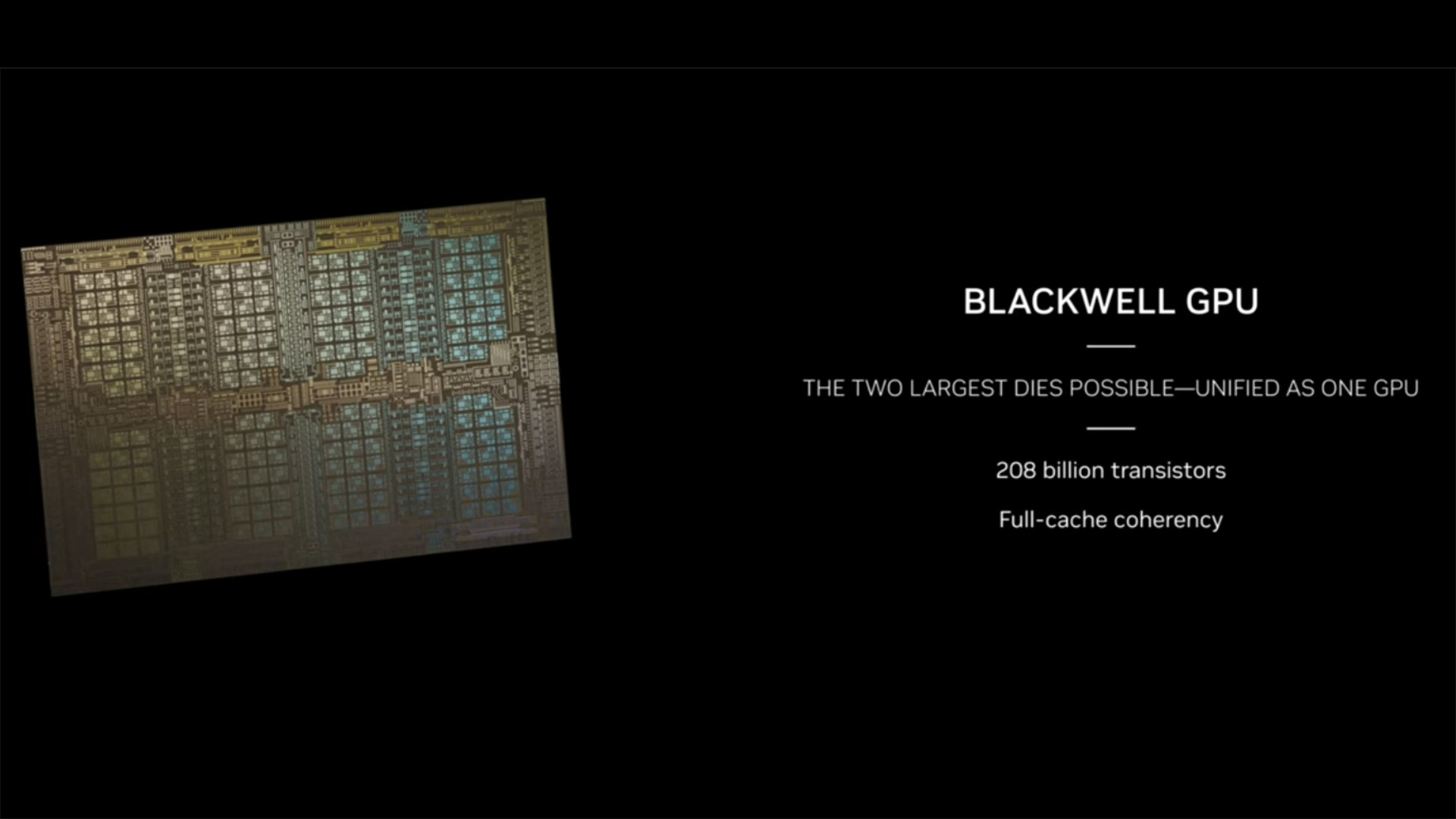
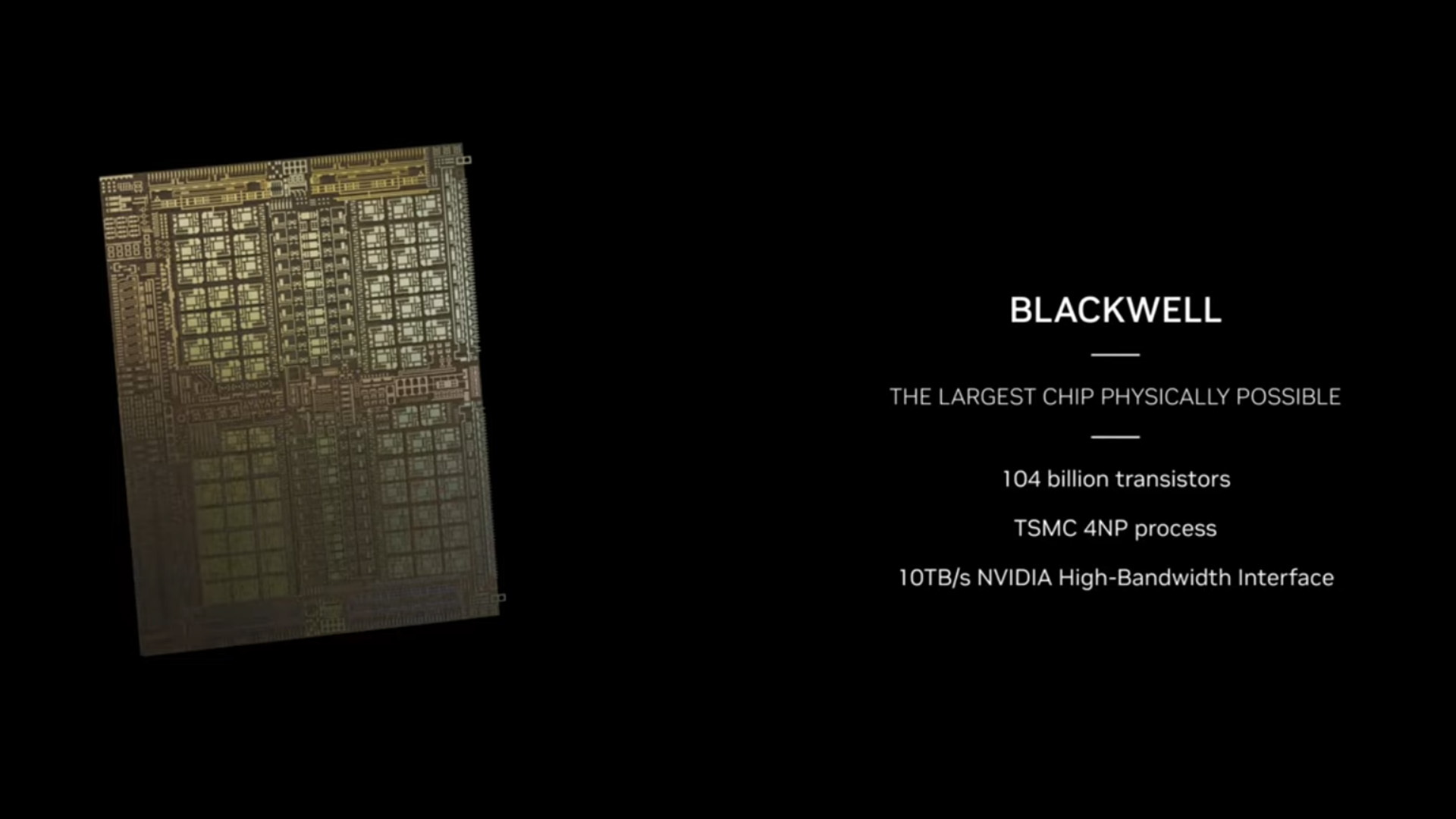
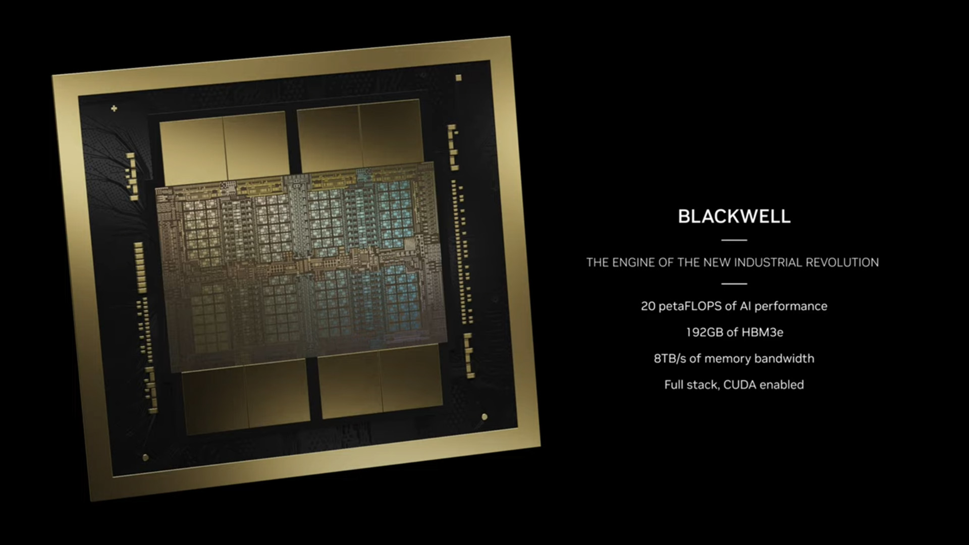
Anyway, if you assume a similar approach with Blackwell, a GB202 chip will need in excess of 175 SMs and therefore well over 100 billion transistors. The problem is that the 104 billion transistor die in the new Blackwell GPU is right at the limit of what is possible with the TSMC 4N process.
That's related to something known as the reticle limit, which dictates the largest possible die size. And Nvidia says the new Blackwell die is at that limit with 104 billion transistors. And some basic maths suggest that an RTX 5090 with 175 enabled SMs would need an even bigger transistor count still.
Moreover, even if 175 enabled SMs could be squeezed into 104 billion transistors, what makes sense for an AI GPU being sold for many tens of thousands of dollars doesn't apply to a gaming GPU that even with a big price hike seems unlikely to go on sale for more than about $2,500. The problem is that a GPU pushed right to the reticle limit by definition means low yields and sky high manufacturing costs. Tolerable for an AI GPU with massive margins, but not at all feasible for a gaming chip.
If that's all accurate, there are two possible solutions. One, Nvidia uses the same dual-die arrangement for Blackwell gaming GPUs as Blackwell AI GPUs. Or option two, Nvidia uses the more advanced TSMC N3 node for the gaming GPUs, allowing a single-die chip well beyond 100 billion transistors.
What doesn't seem plausible right now is a Blackwell gaming GPU with, say, 120 billion transistors in a single chip on TSMC 4NP silicon. What will actually happen, nobody outside of Nvidia knows for sure.
Arguably the most reliable leaker of Nvidia info is twitter account Kopite7kimi. That account claimed yesterday that the GB202 gaming GPU in the RTX 5090 will be on the same silicon process as the new Blackwell AI chip. That makes sense given that TSMC N3 is so new and that it would be a big ask to go with a huge GPU of well over 100 billion transistors on N3 so soon. After all, if N3 was ready for 100 billion-plus transistor GPUs, surely Nvidia would have used it for it new AI chip?
If that's all true, the rumoured information on the RTX 5090 seems to be in some conflict. 175 enabled SMs doesn't seem to compute with TSMC N4 silicon. Unless, that is, the RTX 5090 and GB202 GPU is dual die, just like the Blackwell AI chip.
However, going multi-die is not straight forward. Just because Nvidia can make multi-die work for an AI GPU, it does not follow that it has cracked the problem for gaming graphics where die-to-die latency will be absolutely critical.
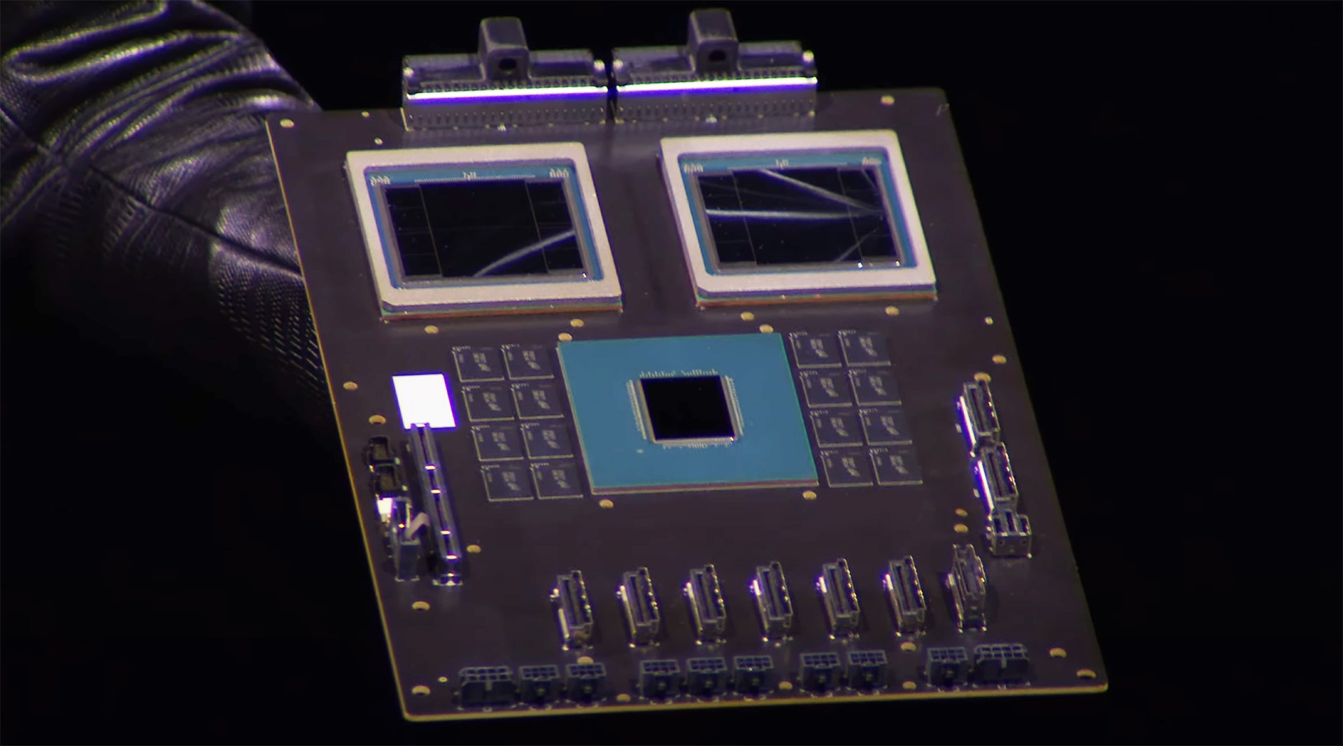
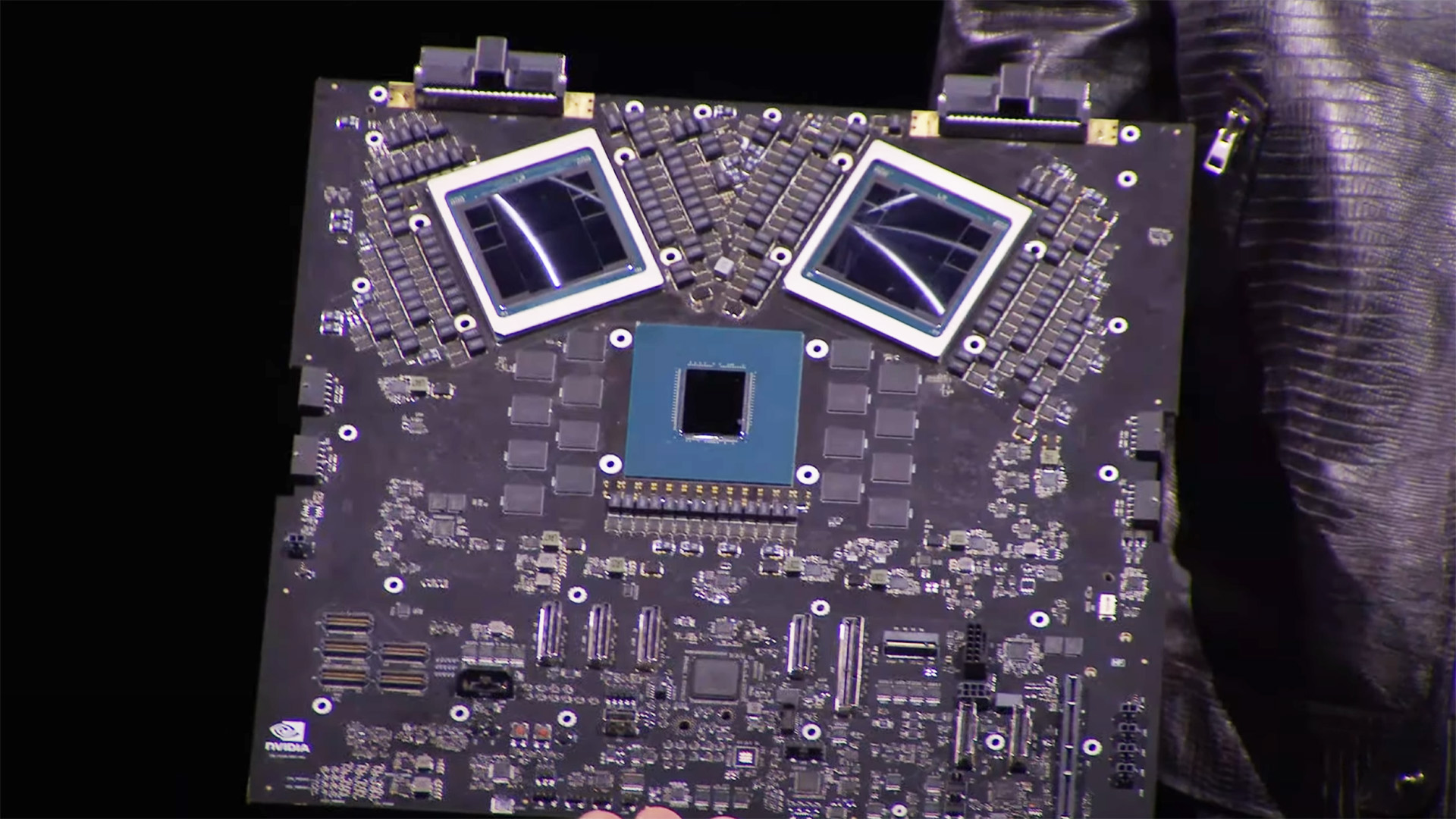
And before anyone suggests that AMD managed it with the Radeon RX 7900 GPUs so why not Nvidia, AMD's multi-die solution is totally different. Where Nvidia has split the computational heart of its Blackwell AI GPU right in half, AMD kept all the actual graphics processing in a single GCD chip. Only the memory controllers and cache were broken out into separate dies.
What's more, rumour has it the whole multi-die thing has proven so difficult for AMD, it's skipping the high-end for its next-gen GPUs in favour of sticking to mid-range cards while it finally gets the multi-die approach sorted for the generation after. Multi-die gaming GPUs, it seems, are very difficult to get right.
Of course, you could argue this is all pretty tangential to most gamers who won't be buying the RTX 5090. Further down the Blackwell gaming stack, for GPUs like the presumed RTX 5060, RTX 5070 and RTX 5080, these problems essentially go away.
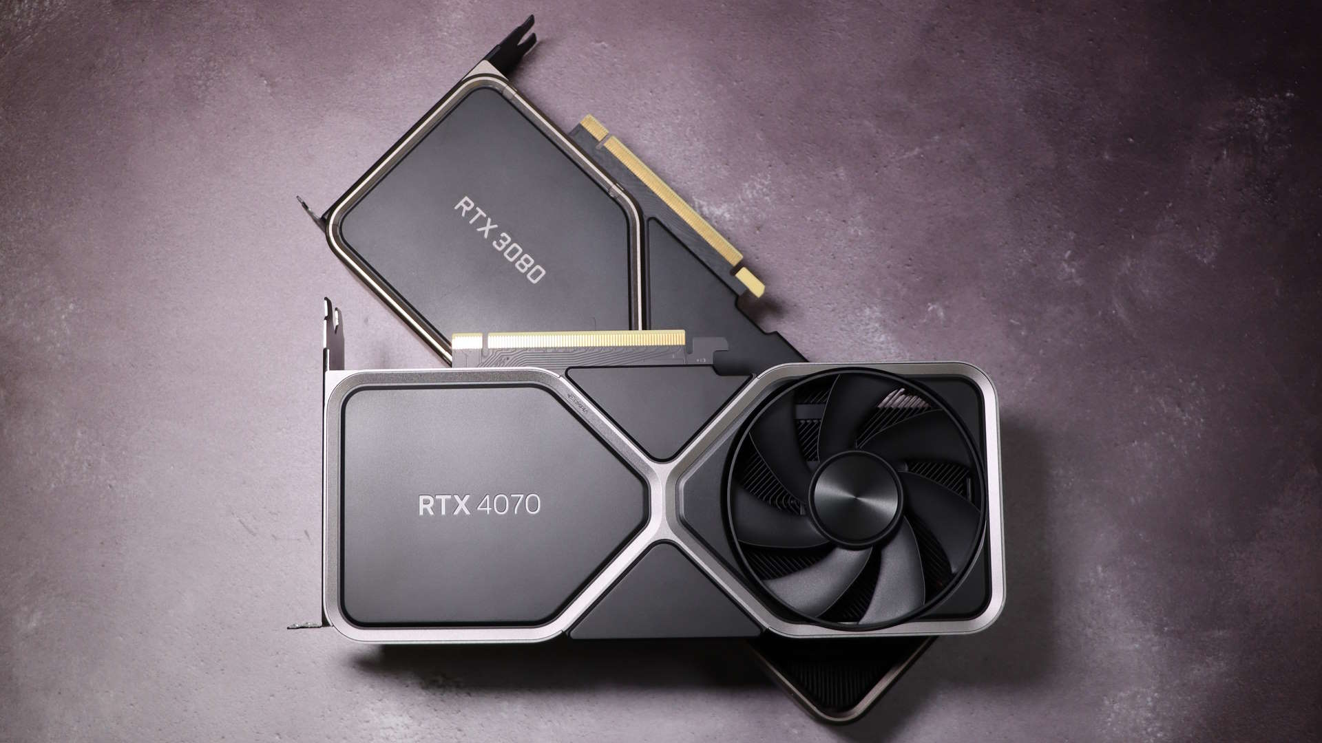
The existing GPU dies in the RTX 4060, 4070 and 4080 series of graphics cards aren't so massive that creating larger and more powerful updates using the Blackwell architecture on TSMC 4NP silicon is implausible.
Best CPU for gaming: The top chips from Intel and AMD.
Best gaming motherboard: The right boards.
Best graphics card: Your perfect pixel-pusher awaits.
Best SSD for gaming: Get into the game ahead of the rest.
Indeed, it's not impossible that Nvidia could even go to Samsung for some of the more mainstream RTX 50-series, albeit Samsung doesn't have a node that can cope with the likes of a 120 billion transistor chip for the RTX 5090.
Anyway, the point is that it's really only the potential RTX 5090 big boi where there seems to be a crunch point involving process nodes, die sizes, and multi-die technology. Can TSMC's 4NP process realistically deliver a 175 SM enabled RTX 5090 on a single die? TSMC N3 might not be ready for such a big chip, either. But then nor is going multi-die easy. Whatever the outcome, the RTX 5090 is going to be very interesting. And very likely hideously expensive. However Nvidia squares this technical circle, it seems like the solution is going to be costly.
As for predictions of what will actually happen, that's a dangerous game. All I'll say is that the RTX 5090 might well have 175 enabled SMs, and it might well be on TSMC 4NP silicon. But if it is both of those things, then it's hard to see how Nvidia pulls that off using a single slice of silicon. Watch this space!


