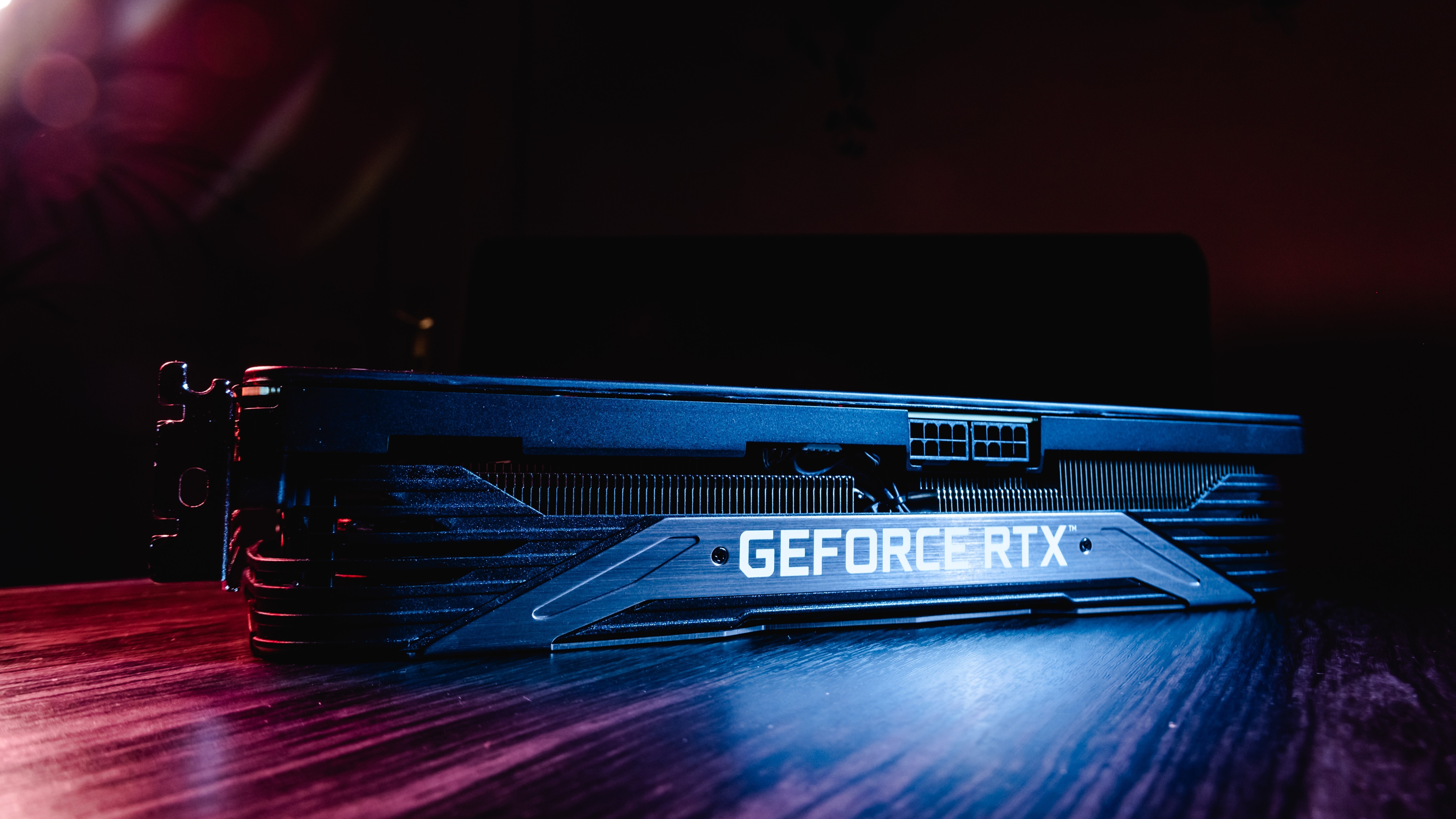
The GeForce RTX 3050 A recently popped up in Nvidia’s GeForce drivers. We could only guess at the specs initially, but now Nvidia has confirmed the GeForce RTX 3050 A’s existence as well as some key specs. We reached out to Nvidia and were informed that the graphics card leverages a down-binned AD106 (Ada Lovelace) silicon and represents the third iteration of the RTX 3050 Laptop GPU, already a questionable choice for mobile use considering the lack of VRAM.
The new RTX 3050 A, where the “A” probably denotes Ada, only uses a fraction of the potential offered by the AD106 die. According to Nvidia, the GPU will feature just 4GB of GDDR6 VRAM on a 64-bit bus along with 1,792 CUDA cores. Power consumption is described as 35-50 watts TGP, which is lower than its 3050 mobile siblings on the top of that range. Many of the available specs for the RTX 3050 A also appear to be lower than the original variant, though there's a catch: We don't have clock speeds for the new part, and Ada tends to clock significantly higher than Ampere.
It’s interesting to see Nvidia switch from the Ampere to the Ada Lovelace for the new RTX 3050 A variant, but it’s a move we’ve seen in the past. For example, a recent RTX 4070 desktop graphics card variant saw Nvidia using down-binned AD103 chips instead of the smaller AD104 GPU. There's also an RTX 2050 laptop chip that uses an Ampere GA107 rather than the expected Turing GPU.
GeForce RTX 3050 A Specifications
The assumption is that Nvidia wants to use every possible piece of silicon by turning off non-functional portions of chips and down-binning them to lower tier parts. For the RTX 3050 A, Nvidia has apparently disabled 61% of the available SMs (Streaming Multiprocessors) and two-thirds of the memory controllers present in the Ada Lovelace AD106 silicon. Some of the disabled bits may have worked, but Nvidia effectively captures just about any potentially useful silicon this way, whether it has 14 or more SMs and two or more memory controllers that are functional.
On paper, then, we’ve got a new mobile GPU that might seem to be slightly less powerful than its RTX 3050 Laptop GPU siblings, but that's only part of the story. The GA107 die normally used in these chips measures 200 mm^2, while the AD106 die measures 188 mm^2. Along with the slight smaller size, the Ada architecture tends to clock significantly higher than Ampere — desktop GPUs typically run in the 2.7 GHz range, compared to 1.9 GHz on Ampere.
We do know from our desktop GPU testing that Ada chips have significantly improved on overall efficiency (FPS per Watt), and there's no reason this down-binned RTX 3050 A won't show similar characteristics — especially if it's running at lower clocks. But we don't have details on clocks speeds as yet, so we can't say for certain what level of performance it may offer. We reached out to Nvidia and were informed that DLSS 3 frame generation will not be supported, even though the OFA (Optical Flow Accelerator) in Ada would normally allow for it.
As noted earlier, it's a common practice for Nvidia and other GPU vendors to use defective chips in lower tier parts. Considering Nvidia doesn't really have a direct alternative to the RTX 3050 A in the 40-series, and since it has far more profitable projects underway, it doesn't make sense to use new wafers on low-end silicon. Instead, it repurposes old stock that may have been destined for the recycling bin. It’s a bit like when your bananas get bruised and your grandma uses them to make banana bread — a delicious and economical way to use what might have ended up in the trash.
We don’t yet know what laptops might use the RTX 3050 A, but it should allow for smaller, thinner designs thanks to Ada's improved efficiency and the chip's smaller size — with just two memory chips instead of the three or four required with the previous models. Just don't expect it to be an amazingly fast gaming solution, as the 3050 Laptop GPU line wasn't exactly a barn burner at launch.


