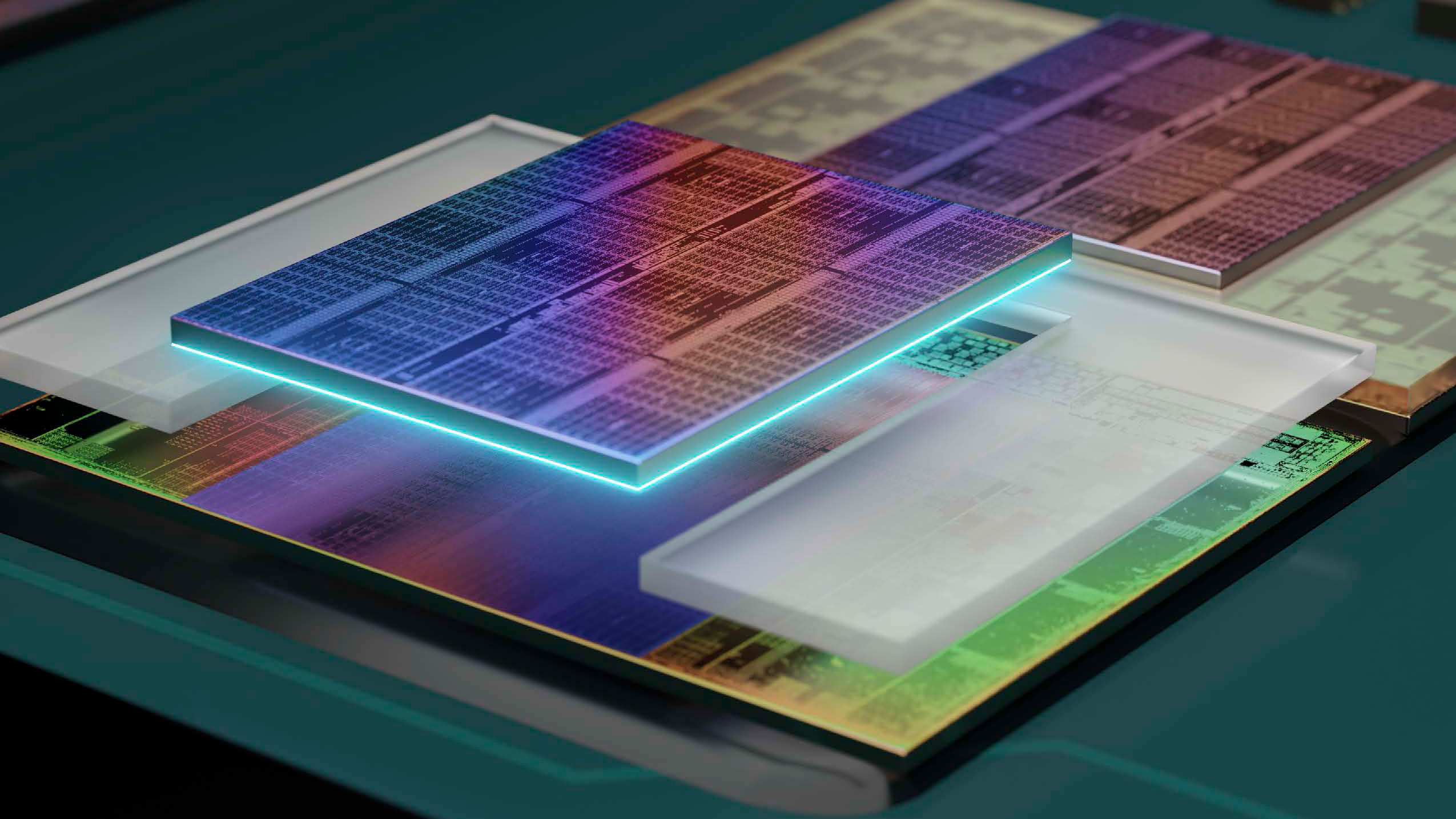
Semiconductor chip building is becoming more complex, and a big trend in that direction is the adoption of new 3D-stacking technologies that improve chip density at a level that would be impossible with traditional shipbuilding methods. A blog post by Nvidia's Baskar Rajagopalan reports that engineering simulation and 3D design software company Ansys is using Nvidia's Omniverse platform to analyze 3D-based semiconductor designs in 3D. The company utilizes Nvidia's modulus Fourier neural operator architecture to predict power profiles when developing chip designs.
This technology is very advantageous for chip designers. Viewing a 3D-based chip design in a 3-dimensional space can give engineers a better perspective of how the chip will behave under various conditions. Nvidia provides an example of finding hot spots and rectifying electromagnetic issues faster and more easily in a 3D-stacked chip design when viewed from a 3-dimensional perspective.