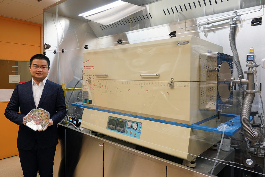
The increasing need for more powerful, faster, and more efficient computing capabilities has been met with increasingly difficult materials and engineering problems as attempts at performance scaling continue. As published on Nature, MIT engineers have developed a new silicon fabrication process that works by depositing three-atom thick, atomically thin transistors (ATTs) on top of already-existing chip circuits – essentially “growing” them into high-density, high-performance computing stacks.
The team’s novel approach looks something like additive manufacturing, and applies a highly uniform, three-atom-thick layer of 2D Transition Metal Dichalcogenide (TMD) materials across an entire 8-inch, fully fabricated silicon wafer. Each new layer of TMD enables denser integrations between the underlying chip and the added transistor stacks, improving performance with unparalleled density.
The base 2D material, molybdenum disulfide, is a flexible and transparent material that ticks all the right boxes when it comes to electrical and photonic conductivity, making it a prime candidate for building semiconductor transistors. It’s composed of a one-atom layer of molybdenum, sandwiched between two atoms of sulfide.
That’s all that’s required to fabricate a modern transistor: three atoms.
That’s the point at which the scaling benefits really start to show, as according to Jiadi Zhu, an electrical engineering and computer science graduate student and co-lead author of the paper on this new technique. “Using 2D materials is a powerful way to increase the density of an integrated circuit. What we are doing is like constructing a multistory building. If you have only one floor, which is the conventional case, it won’t hold many people,” Zhu told MIT News. “But with more floors," he added "the building will hold more people that can enable amazing new things. Thanks to the heterogenous integration we are working on, we have silicon as the first floor and then we can have many floors of 2D materials directly integrated on top.”
Some crucial updates make this new design process “grow” as a possible venue for future chip fabrication. Usually, growing or depositing 2D layers onto a CMOS wafer requires temperatures around 600 degrees Celsius. The problem here is that silicon circuits tend to break down when subject to temperatures of 400 degrees Celsius or more.
Importantly, the new “growth” process designed by the MIT team was developed with these constraints in mind. They developed a dual chemical vapor deposition process that features two chambers operating at different temperatures: the molybdenum precursor stays in the low-temperature region of the chambers (which stays below 400 degrees Celsius threshold that’s damaging for electronic circuits), while the sulfur flows through the high-temperature region (above 550 degrees Celsius), decomposing, which allows it to later react with the molybdenum in the TMD deposition process.
Another innovation is that for the first time, it’s possible to “grow” the atomically thin transistors as a single unbroken layer across the entire destination chip or wafer. Past techniques (and their limitations) led to processes that had researchers grow the layers on a different medium, transferring them onto the chip itself later on in the process. This often caused imperfections, as the layer didn’t perfectly overlay with the silicon chips that were their destination. And you can imagine the difficulty in aligning the nearly atom-thin structures of the chip with the layers themselves.
Through the various process improvements achieved by the MIT engineers, which leveraged the state-of-the-art MIT.Nano facilities, the researchers managed to demonstrate high levels of layer uniformity and quality at the 8-inch wafer scale required for modern manufacturing processes. The work now shifts to being able to fine-tune the technique and increase the number of stacked transistor layers while exploring alternative, flexible deposition surfaces that could be turned into a microcircuit, such as polymers, textiles, or even paper (think processing-enabled notebooks, clothing, and other applications).


