
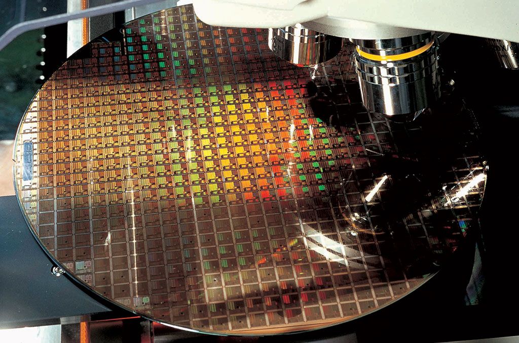
With smaller process nodes becoming increasingly more expensive to achieve, chip manufacturing engineers are turning to other ways to increase the number of transistors that can be packed into a single die. In some ways similar to traditional chip stacking, one research team has created a way to implement an extra layer of microscopic switches on an already completed die, by sticking them where the power and signals go.
Okay, so that's a very rough description of the work conducted by MIT's Department of Electrical Engineering and Computer Science, the University of Waterloo, and Samsung Electronics. But when you read the details about it in the press release on the matter, you'll see that it's a tad difficult to describe it all in just one sentence.