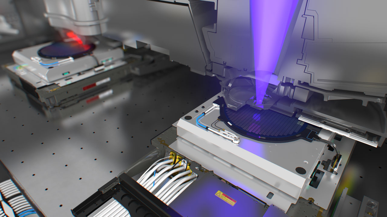
Japan's National Institute of Advanced Industrial Science and Technology (AIST) is partnering with Intel to establish a new research and development center focused on advanced chip production, reports Nikkei citing sources with knowledge of the matter. This facility is expected to be operational within three to five years and will focus on process technologies that use EUV lithography.
The new R&D center will cost hundreds of millions of dollars (as each EUV litho machine costs around $200 million) and will provide an opportunity for various industry players in Japan to collaborate with AIST and Intel by jointly using EUV equipment for prototyping and testing. The move will enable chip designers in Japan to adopt the latest process technologies, such as those relying on EUV tools, which will ultimately make them more competitive with industry peers based elsewhere.