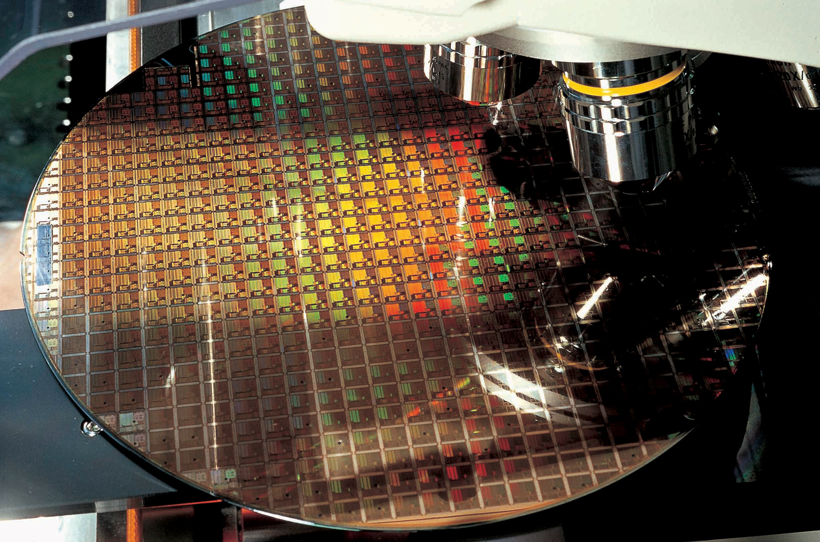
TechInsights and SemiWiki have published key details that Intel and TSMC disclosed about their upcoming 18A (1.8nm-class) and N2 (2nm-class) process technologies at the International Electronic Devices Meeting (IEDM). According to TechInsights, Intel's 18A could offer higher performance, whereas TSMC's N2 may provide higher transistor density.
Analysts at TechInsights believe that TSMC's N2 offers a high-density (HD) standard-cell transistor density of 313 MTr/mm^2, which far exceeds the HD cell density of Intel's 18A (238 MTr/mm^2) and Samsung's SF2/SF3P (231 MTr/mm^2). While the information more or less aligns with SRAM cell sizes for 18A, N2, and N3, as well as with TSMC's expectations for N2 and N3, there are some things to note.