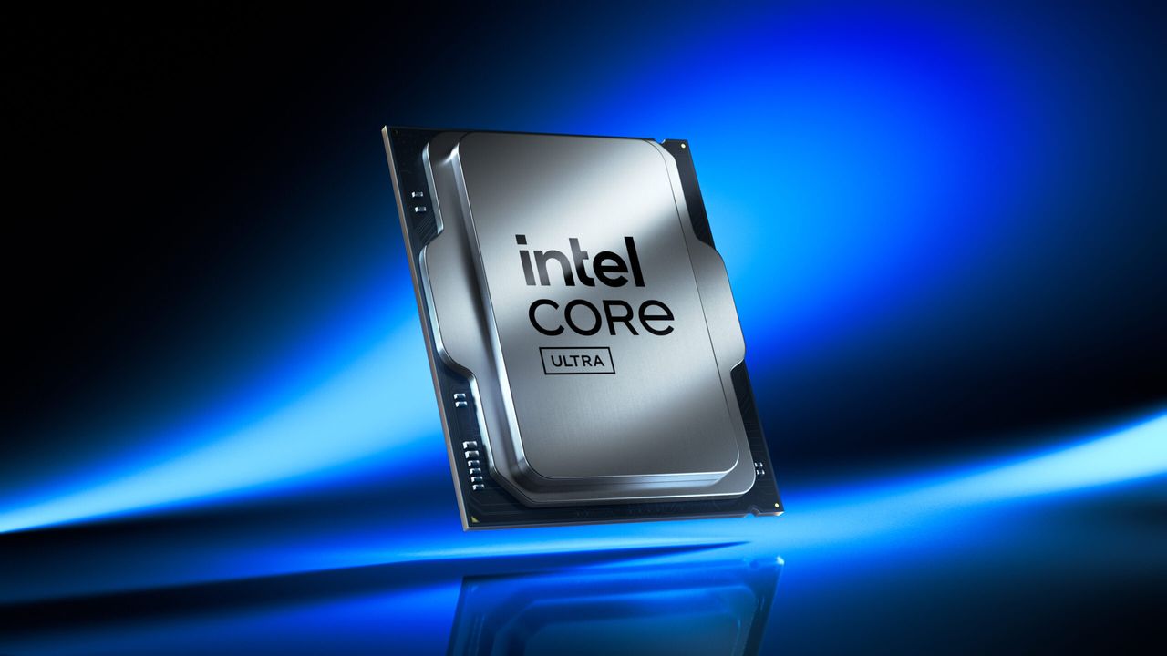
Intel expects its Core Ultra series 4 processors, codenamed Nova Lake, to change its fortunes on the desktop and laptop markets and finally offer performance that is higher compared to direct competitors from AMD. However, another important factor to consider will be the costs of these CPUs, and if the alleged Nova Lake compute chiplet die sizes leaked by @9550pro are accurate, these processors will be anything but cheap to make.
When implemented on TSMC's N2 manufacturing technology, Nova Lake's compute tile with eight high-performance Coyote Cove P-cores and 32 energy-efficient Arctic Wolf E-cores measures over 110 mm^2, whereas the same tile equipped with 144 MB of big last-level cache (bLLC) measures over 150 mm^2, if the numbers from @9550pro are correct. To put the number into context, it is believed that the size of Arrow Lake's compute tile —implemented on TSMC's N3B technology and housing eight Lion Cove P-cores and 16 Skymont E-cores — is believed to be around 117 mm^2.
TSMC's N2 is projected to be a more expensive process technology to use than N3B, as, despite the fact that it is expected to feature roughly the same number of EUV layers (20 ~ 23), it is also believed to use EUV multipatterning for at least some critical layers, which adds costs. This, and other factors, contribute to manufacturing costs, so it is safe to say that Nova Lake's compute tile without bLLC will be a bit more expensive to make than Arrow Lake's compute tile, assuming an accurate die size for the former. The compute tile with bLLC will be significantly more expensive, though, considering that these tiles will be used for expensive CPUs aimed at gamers and enthusiasts, this will hardly be a problem for Intel.
Just like most of Intel's latest processors in recent years, Nova Lake will use a multi-tile design that will include a compute tile (or two), a system-on-chip (SoC) tile, a GPU tile, an I/O tile, and a base tile. The main chiplet — the compute tile — will be made using both Intel's own 18A fabrication technology at the company's Fab 32 in Arizona as well as TSMC's N2 manufacturing process at the foundry's Fab 22 in Taiwan.
Intel has never publicly revealed which versions of Nova Lake will be used for desktops and which will be used for laptops, and whether there will be any difference at all. However, given that Intel expects to make the majority of Nova Lake silicon in-house and keeping in mind that laptop CPUs outsell desktop CPUs 7:3 these days, it is reasonable to expect that the bulk of laptop CPUs will be made at Intel's own fab in Arizona. To that end, the company's balance sheet will barely suffer from the high costs of its Nova Lake compute tiles with bLLC at TSMC.
The cost of a chip is a function of process technology, die size, functional yield, and parametric yield. While we may well speculate that TSMC's N2 is more expensive than N3B, without factors like parametric yields, our assumptions about the costs of the actual compute tile will be highly speculative, to put it mildly.

Follow Tom's Hardware on Google News, or add us as a preferred source, to get our latest news, analysis, & reviews in your feeds.