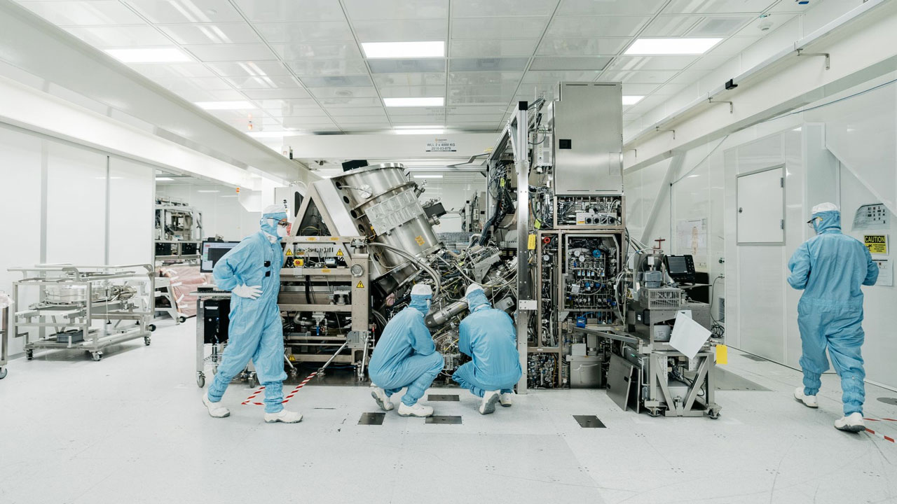
Intel has started using two leading-edge ASML High-NA Twinscan EXE:5000 EUV lithography tools, the company revealed on Monday at an industry conference, Reuters reports. The company uses these systems for research and development purposes, and so far, Intel has processed tens of thousands of wafers using them.
Intel installed and started using two High-NA EUV lithography tools from ASML at its D1 development fab near Hillsboro, Oregon, last year and has now processed as many as 30,000 wafers using these systems, Intel engineer Steve Carson revealed at the SPIE Advanced Lithography + Patterning conference. Intel was the first leading chipmaker to get High-NA EUV machines (which are believed to cost €350 million each) last year and plans to use them to produce its 14A (1.4nm-class) chips several years down the road.