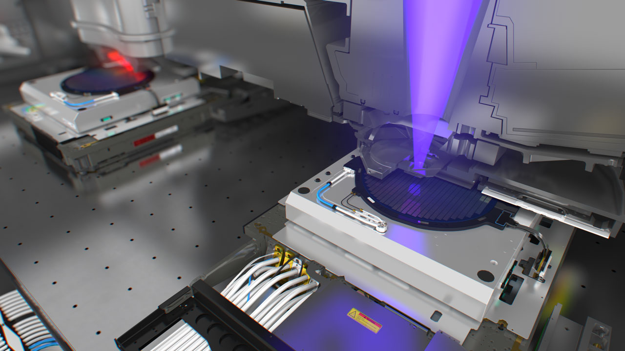
ASML and Intel said this week that the latter had achieved a significant milestone with ASML's High-NA lithography system by turning on its light source and making the light reach resist on a wafer, according to a report from Reuters. This indicates that the light source and mirrors are aligned correctly, a critical step in the bring-up process. This 'first light' milestone indicates that one of the main components of the Twinscan EXE:5000 system is operational, though not yet at peak performance.
ASML's Twinscan EXE High-NA EUV litho machines with projection optics featuring a 0.55 numerical aperture can achieve resolution of down to 8nm with a single exposure — down from typical Low-NA EUV systems that offer a 13.5nm resolution with a single exposure. The first of these systems is currently housed at ASML's laboratory in Veldhoven, Netherlands, while a second is being assembled at an Intel facility near Hillsboro, Oregon.
"Technically, this 'first light' actually is 'first light on the wafer,'" explained Marc Assinck, a spokesman for ASML. "The light source was already working, now we have the photons 'in resist' on the wafer."
ASML specialists are still calibrating the High-NA tool in the Netherlands, so the machine yet has to print its first test patterns.
The development was initially disclosed by Intel's Ann Kelleher at the ongoing SPIE lithography conference in San Jose, California. Intel is currently assembling its first Twinscan EXE:5000 lithography machine at its site near Hillsboro, Oregon. The machine will be used primarily for process development purposes when it is assembled several months down the road.
In a recent test, the Veldhoven machine successfully demonstrated its capabilities on a silicon wafer prepared with photoresists, indicating its readiness for circuit pattern printing. This achievement, referred to as 'first light on the wafer' marks a significant step forward in the field of High-NA EUV lithography.
High-NA EUV lithography is anticipated to be adopted by leading chipmakers, including Intel, Samsung, and TSMC, within the next few years. Intel has already expressed intentions to utilize the system for its upcoming Intel 14A node-based generation of chips.
Light source is among the most complex part of any extreme ultraviolet (EUV) lithography tools. Neither ASML nor Intel disclose maximum performance (wattage) of Twinscan EXE's light source.


