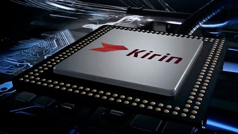
Huawei has announced a new chip design framework aimed at closing the technology gap with global semiconductor leaders like TSMC and Nvidia, targeting '1.4nm-class' transistors and a 55% increase in transistor density. The firm also unveiled a new 'Tau Scaling Law' that's designed to replace Moore's Law for future chip scaling. Unveiled at the IEEE International Symposium on Circuits and Systems (ISCAS 2026) in Shanghai on Monday, this new design method is intended to circumvent strict US trade sanctions. It allows the company to develop high-performance smartphones and AI processors without relying on restricted Western manufacturing equipment like extreme ultraviolet (EUV) lithography machines.
Delivering a keynote address at the symposium, He Tingbo — a Huawei board member and President of its semiconductor division, HiSilicon — unveiled the company's new, proprietary “LogicFolding” architecture. The cutting-edge design blueprint is built directly upon the newly introduced Tau Scaling Law.