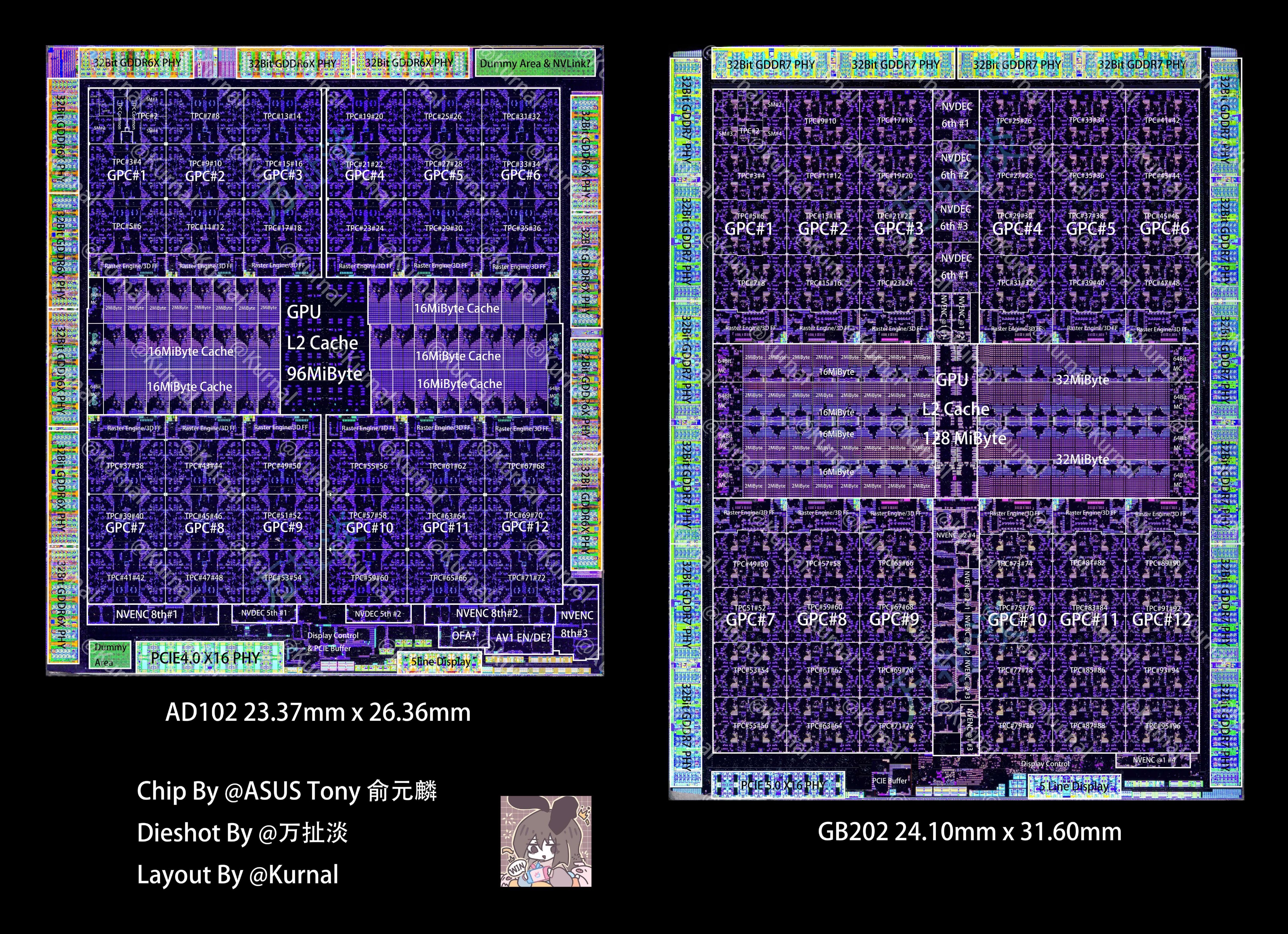
A diagram of Nvidia's flagship GB202 die, which powers the RTX 5090, was shared on X, revealing the componentry layout of Nvidia's Blackwell architecture. The image annotated by Kurnal shows the layout of GB202's primary components, such as the L2 cache, GPCs, SMs, memory controllers, and more. A second image was also shared comparing GB202 to AD102, used with Nvidia's previous-gen RTX 4090 flagship.
Looking at the GB202 die shot, the L2 cache resides directly in the middle of the die, split into several 2 MB chunks, forming two 32 MB layers. Surrounding the entire L2 cache pool are 12 graphics processing clusters. Inside each cluster resides several texture processing clusters responsible for vertex shading, texture mapping, and rasterization. Inside each TPC are several Streaming Processors that contain components such as the GPU's CUDA cores and L1 cache. There are 96 TPCs, with each TPC allegedly having up to four SMs each.