
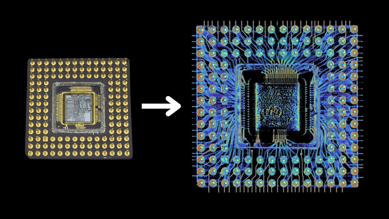
In today's world of bleeding-edge processes and packaging techniques, the Intel 386 doesn’t look like much—a grey ceramic slab with 132 gold pins, something you’d expect to find rattling around in an old parts bin at this point. But behind that dull façade lies a marvel of late-1980s chip packaging, the kind of engineering we've taken for granted. Using a CT scanner and some clever digital dissection, Ken Shirriff managed to explore every layer of this classic CPU without once touching a screwdriver or desoldering gun.
The scan produced hundreds of razor-thin X-ray slices, which were stitched into a 3D model you can spin, zoom, and digitally “peel” layer by layer. The first reveal is a halo of gold bond wires, each just 35 µm thick, far thinner than a human hair, radiating from the silicon die. These act as microscopic suspension bridges between the die’s pads and the package’s internal routing. Some carry simple data or control signals, others gang together—up to five on a pad—to handle the heavier demands of power and ground.