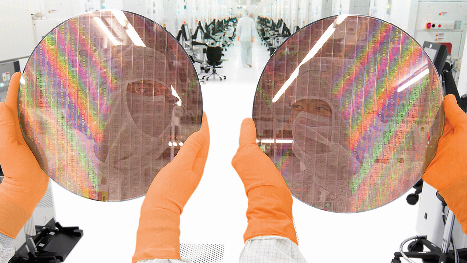
SK hynix is evaluating Tokyo Electron's (TEL) latest cryogenic etching tools, which operate at -70C temperatures, to enable new flavors of 3D NAND with more than 400 layers. Cryogenic etching tools 'drill holes' three times faster than conventional tools, a capability that will be instrumental for 3D NAND with over 400 active layers, reports The Elec.
Instead of importing the actual equipment to South Korea, SK hynix is sending test wafers to Tokyo Electron labs in Japan. This method enables the 3D NAND maker to effectively assess the technology's potential without shipping actual tools to SK Hynix and installing them into fabs. The new etching system operates at a chilling temperature of -70°C, which is a stark contrast to the 0°C to 30°C range of current etching processes.
The report says TEL's next-generation etching machine can make a 10-µm-deep etch with a high aspect ratio in just 33 minutes, over three times faster than existing tools. This achievement is not only a major technical improvement but also greatly increases 3D NAND production efficiency, which could reshape the production timelines and output quality of 3D NAND devices.
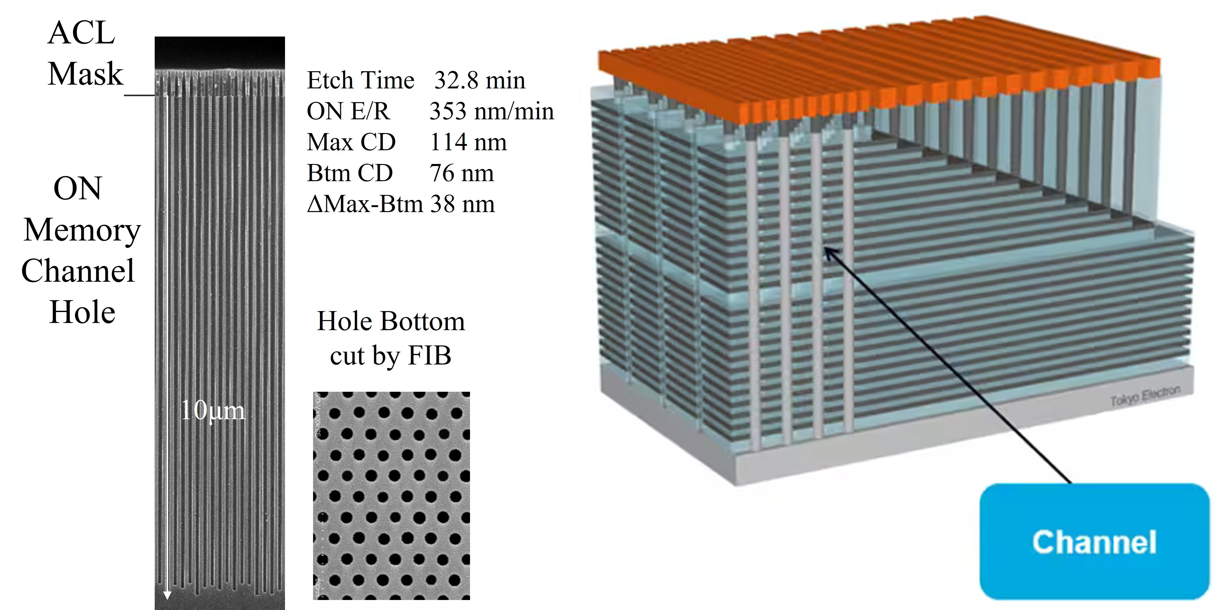
When it comes to producing 3D NAND, some may say that 'etching vertical holes' is simple — but it is not. In fact, etching deep memory channel holes with good uniformity is a challenge, which is why the industry has adopted double stacking and even triple stacking (building two or three separate stacks instead of one with a 'deep' channel hole) for 3D NAND.
SK hynix's 321-layer 3D NAND products are said to use a triple-stack structure. With the adoption of TEL's new etching equipment, it will be possible to build a 400-layer 3D NAND device in a single or double stack, which means higher production efficiency. The decision on whether future products with more than 400 layers will transition to a single or double stack will depend on how reliably the tool performs and whether it can reproduce its results consistently.
A significant environmental advantage of TEL’s equipment is its use of hydrogen fluoride (HF) gas, which has a global warming potential (GWP) of less than 1. This is a drastic reduction compared to the traditionally used perfluorocarbons like carbon tetrafluoride (CF4) and octafluoropropane (C4F8), which have GWPs of 6030 and 9540, respectively. As a result, the potential adoption of TEL's new tool reflects a growing industry trend towards greener manufacturing practices.
While SK hynix is testing the etching tool by sending wafers to Tokyo Electron, Samsung Electronics is concurrently evaluating the same technology by importing a demo version of the tool. The results of these tests will determine the future adoption and potential standardization of cryogenic etching technologies in semiconductor manufacturing in general.